Method for fabricating semiconductor device with use of partial gate recessing process

a semiconductor device and recessing technology, applied in the field of semiconductor device fabrication, can solve the problems of reducing the resistance of the gate electrode sheet, affecting the reliability of the gate dielectric layer b>12/b>, and achieving the effect of preventing mechanical stress

Inactive Publication Date: 2006-07-11
SK HYNIX INC
View PDF3 Cites 9 Cited by
  • Summary
  • Abstract
  • Description
  • Claims
  • Application Information

AI Technical Summary

Benefits of technology

[0018]Consistent with the present invention , there is provided a method for fabricating a semiconductor device with a polymetal gate electrode capable of preventing a mechanical stress induced from a hard mask during a high thermal annealing process.

Problems solved by technology

However, the tungsten polycide gate electrode has a very high value of resistivity, and thus, it is limited in reducing a sheet resistance of a gate electrode.
However, this relatively high temperature may induce a mechanical stress originated from the hard mask 15, and this induced mechanical stress subsequently causes reliability of the gate dielectric layer 12 to be deteriorated.

Method used


Image

  • Method for fabricating semiconductor device with use of partial gate recessing process
  • Method for fabricating semiconductor device with use of partial gate recessing process
  • Method for fabricating semiconductor device with use of partial gate recessing process

Examples


Embodiment Construction

[0026]Hereinafter, a method for fabricating a semiconductor device with use of a partial gate recessing process in accordance with an embodiment of the present invention will be described in detail with reference to the accompanying drawings.

[0027]FIGS. 3A to 3G are cross-sectional views illustrating a method for fabricating a semiconductor device in accordance with an embodiment of the present invention.

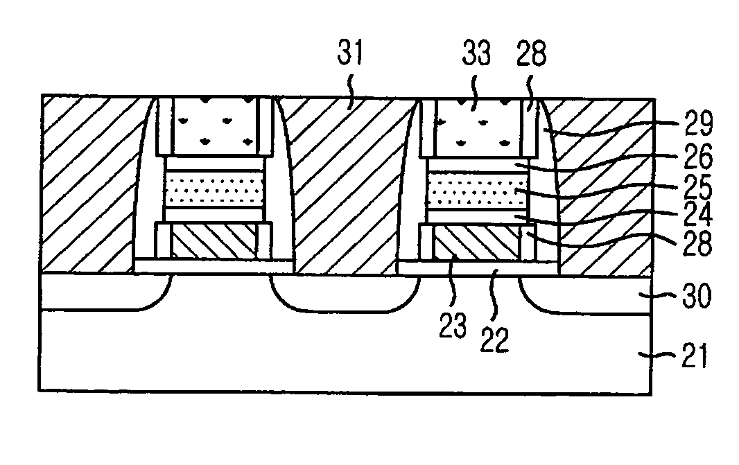
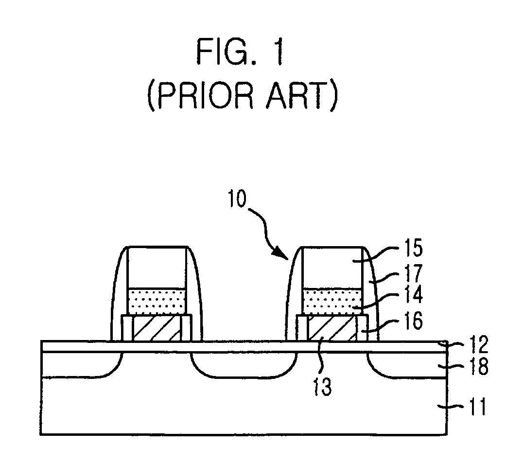
[0028]Referring to FIG. 3A, a gate dielectric layer 22 is formed on a substrate 21. Although not illustrated, the substrate 21 is provided with a device isolation region and a well by performing an ion implantation process. Then, a polysilicon layer 23, a diffusion barrier layer 24, a tungsten layer 25, an etch stop layer 26, and a sacrificial layer 27 are sequentially formed on the gate dielectric layer 22.

[0029]At this time, the polysilicon layer 23 is doped with one of N-type dopants and P-type dopants and has a thickness ranging from approximately 200 Å to approximately 800 Å. T...


PUM


Abstract

Disclosed is a method for fabricating a semiconductor device with a polymetal gate electrode formed by a partial gate recessing process. The method includes the steps of forming a gate structure including a gate dielectric layer, a polysilicon layer, a metal layer, an etch stop layer and a sacrificial layer sequentially formed on a substrate; selectively performing a re-oxidation process to the gate structure; forming a spacer on each sidewall of the gate structure; implanting ions in the substrate for forming source / drain regions; selectively removing the sacrificial layer of the gate structure to form a recess; and filling an insulating hard mask into the recess for use in a self-aligned contact etching process.

Description

[0001]The present application relates to and claims priority from Korean patent application No. KR 2003-0076032, filed in the Korean Patent Office on Oct. 29, 2003, the entire contents of which are incorporated herein by reference.[0002]1. Field of the Invention[0003]The present invention relates to a method for fabricating a semiconductor device; and, more particularly, to a method for forming a transistor with a polymetal gate electrode.[0004]2. Description of Related Arts[0005]Recently, as the design rule of a metal oxide semiconductor field effect transistor (MOSFET) has been rapidly scaled down to the size of about 90 nm, a linewidth of a gate electrode, a thickness of a gate dielectric layer, and a depth of a source / drain junction have been also decreased in order to meet the recent demand. Particularly, it is highly mandated to develop a gate electrode with a low resistance to solve a problem of a resistance-capacitance (RC) delay.[0006]Therefore, a study on a stack gate elec...

Claims


Application Information

Patent Timeline
Patent Type & Authority Patents(United States)
IPC IPC(8): H01L21/8234H01L21/28H01L21/336H01L29/49
CPCH01L21/28061H01L21/823437H01L29/6656H01L29/66545H01L29/4941H01L21/18
Inventor CHO, HEUNG-JAEJANG, SE-AUGLIM, KWAN-YONG
Owner SK HYNIX INC
Why Eureka
Try Eureka