Semiconductor device and manufacturing method thereof

a technology of silicon semiconductor and thin film, which is applied in the direction of transistors, basic electric elements, thermoelectric devices, etc., can solve the problems of sputtering apparatus, low throughput, and high cost of silicon semiconductor production using such a technology, and achieve the effect of reducing contact resistance, increasing electric current of organic tft of bottom contact type, and low cos

Inactive Publication Date: 2006-07-25
HITACHI LTD
View PDF4 Cites 32 Cited by
  • Summary
  • Abstract
  • Description
  • Claims
  • Application Information

AI Technical Summary

Benefits of technology

[0014]Owing to the present invention, the amount of electric current of a bottom-contact type organic TFT can be increased so as to be equal to that of a-Si TFT by reducing contact resistance made on the boundary surface between electrode and semiconductor of the bottom-contact type organic TFT. Therefore, semiconductor devices such as display devices, ID tags, sensors and the like can be provided at low cost.

Problems solved by technology

However, the production of TFT using such a silicon semiconductor entails a great cost because it requires a plasma chemical vapor deposition (CVD) apparatus, a sputtering apparatus and the like, which are expensive.
Moreover, the TFT is produced through many processes such as vacuum process, photolithography, processing, etc., resulting in a low throughput.
It is known that organic semiconductor materials are generally inferior to inorganic semiconductors in chemical resistance and heat resistance.
Therefore, in the case of organic TFT comprising a mixture of an organic semiconductor, a metal for electrodes, and another organic material for an insulating film or the like, an organic semiconductor film is liable to be deteriorated during a process of forming individual layers.
As a result, there is the following problem: a large number of grain boundaries are present in a channel region near the boundary between each of the source and drain electrodes and the semiconductor, so that the contact resistance on the boundary surface between each of the source and drain electrodes and the semiconductor is increased.
Moreover, when the gold electrode is modified with molecules with a large molecular length of octadecanethiol or the like, the distance between gold and pentacene is increased, so that the injection of carriers into the semiconductor from the electrode is undesirably disturbed.

Method used


Image

  • Semiconductor device and manufacturing method thereof
  • Semiconductor device and manufacturing method thereof
  • Semiconductor device and manufacturing method thereof

Examples


example 1

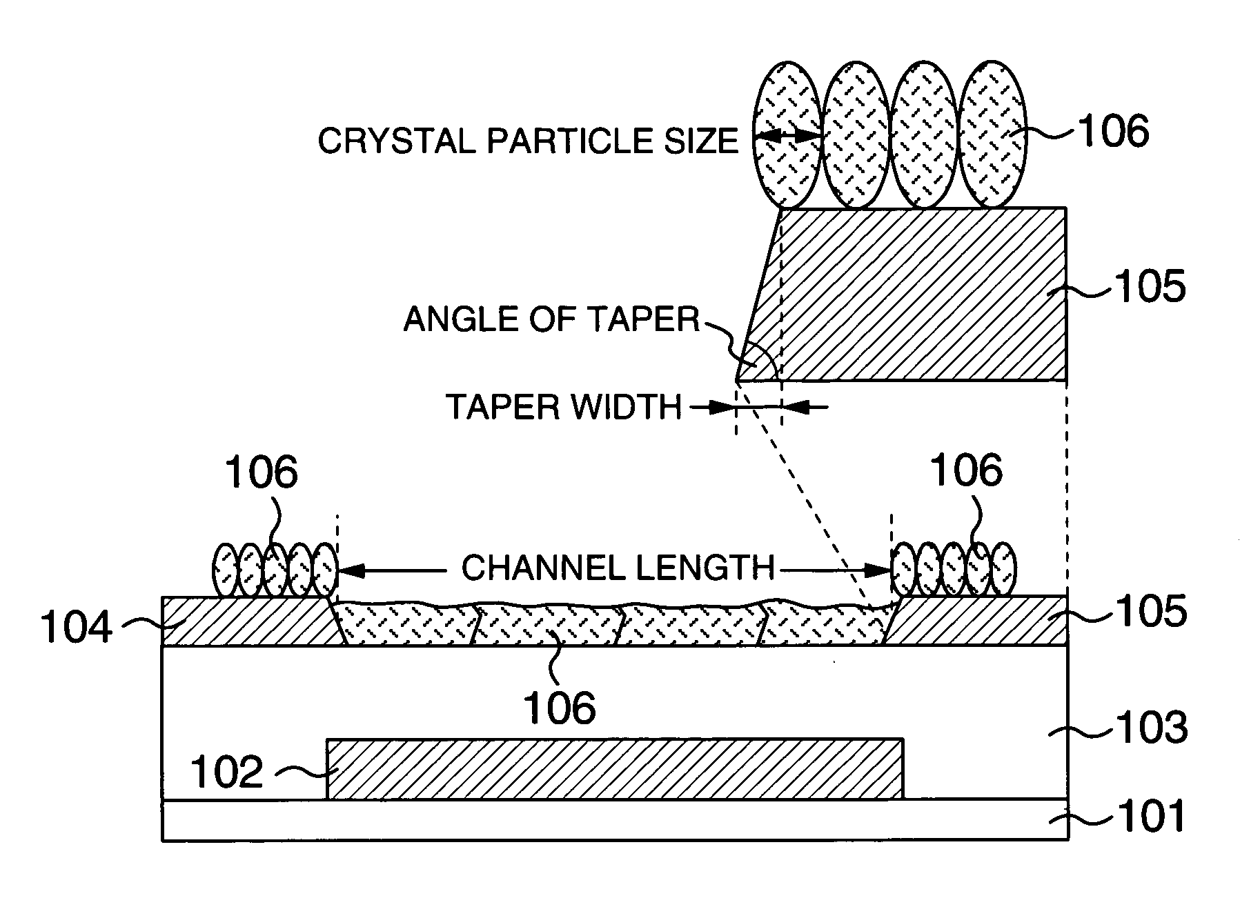
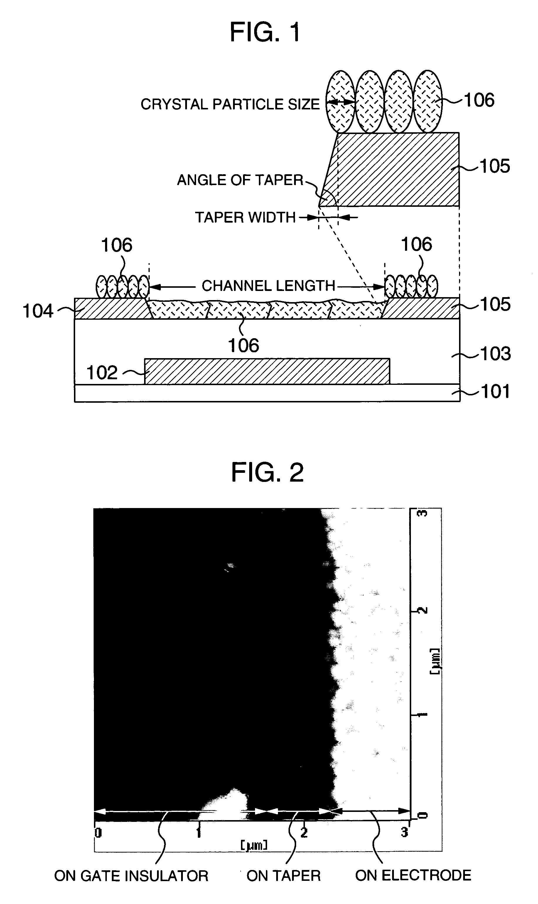
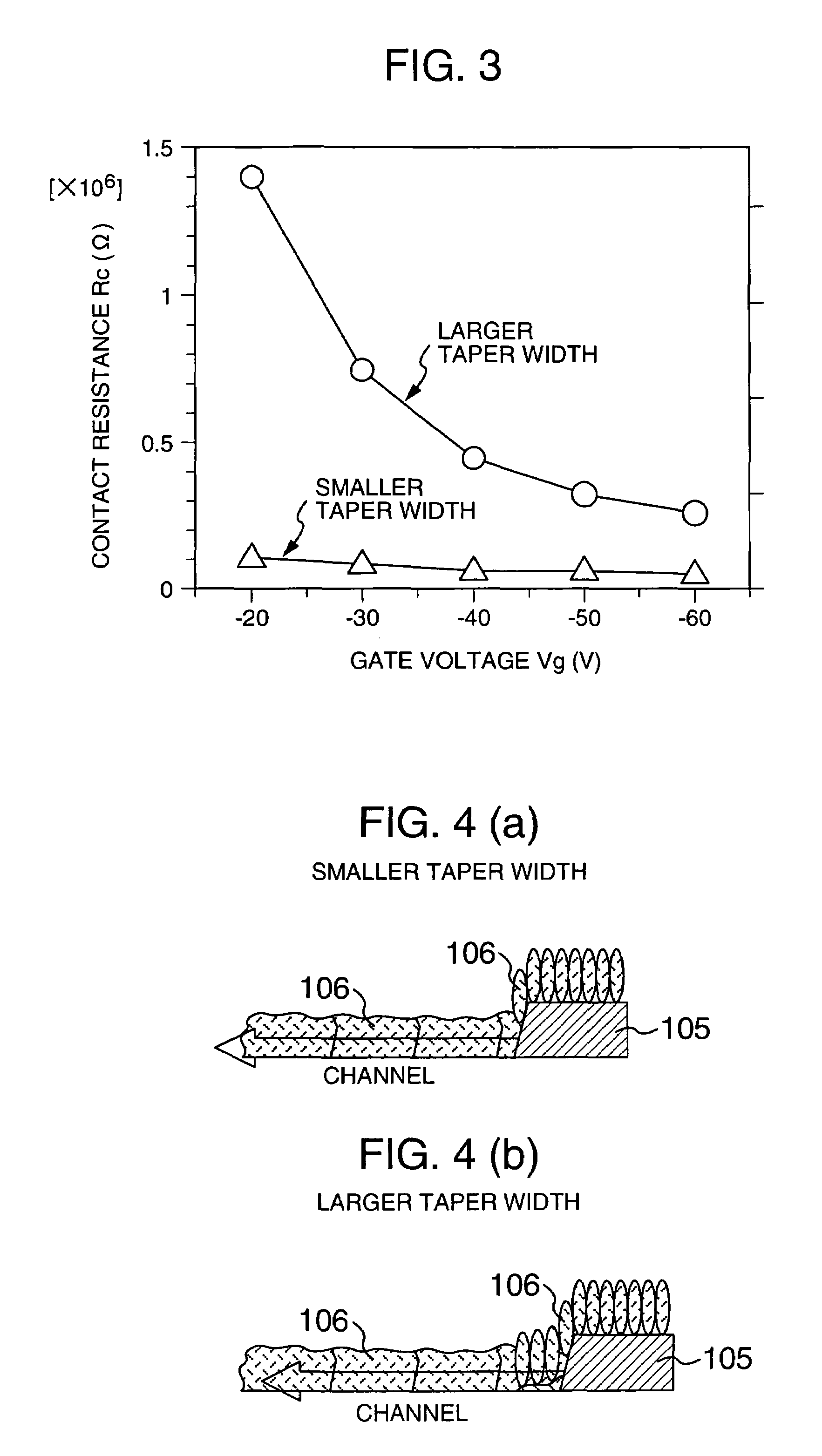
[0027]A first example of the present invention is explained below with reference to FIGS. 1 to 4. FIG. 1 is a schematic cross-sectional view of a bottom contact type organic TFT obtained according to the present invention. A glass substrate was used as an insulating substrate 101, and a chromium film of 100 nm in thickness was formed on the glass substrate by sputtering. Then, a gate electrode 102 was formed by photolithography. A material for the insulating substrate 101 may be selected from various materials so long as it is an insulating material. Specifically, there may be used, for example, inorganic materials such as glass, quartz, alumina sintered product, etc.; insulating plastics such as a polyimide film, polyester film, polyethylene film, polyphenylene sulfide film, poly(p-xylene) film, etc; and hybrid substrates obtained by combining any of these inorganic materials and any of these insulating plastics. As the gate electrode 102, there may be used metals such as tantalum,...

example 2

[0031]A second example of the present invention is explained below with reference to FIG. 5 and FIG. 6. FIG. 5 is a schematic cross-sectional view of a second example of the semiconductor device of the present invention. A glass substrate was used as an insulating substrate 101, and a chromium film of 100 nm in thickness was formed on the glass substrate by sputtering. Then, a gate electrode 102 was formed by photolithography. As in the first example, a material for the insulating substrate 101 may be selected from various materials so long as it is an insulating material. As the gate electrode 102, other metals, alloys obtained by using these metals, electroconductive polymers and the like may be used as in the first example. As a method for forming the gate electrode 102, any of ink jet, a printing method, and photolithography may be employed. Next, a SiO2 film of 300 nm in thickness was formed by CVD to form a gate insulator 103. The gate insulator 103 may also be formed in the s...

example 3

[0032]A third example of the present invention is explained below with reference to FIGS. 7 to 10. FIG. 7 is a schematic cross-sectional view of a third example of the semiconductor device of the present invention. A glass substrate was used as an insulating substrate 101, and a chromium film of 100 nm in thickness was formed on the glass substrate by sputtering. Then, a gate electrode 102 was formed by photolithography. As in the first embodiment, a material for the insulating substrate 101 may be selected from various materials so long as it is an insulating material. As the gate electrode 102, other metals, alloys obtained by using these metals, electroconductive polymers and the like may be used as in the first embodiment. As a method for forming the gate electrode 102, any of ink jet, a printing method, and photolithography may be employed. Next, a SiN film of 300 nm in thickness was formed by CVD to form a gate insulator 103. The gate insulator 103 may also be formed in the sa...


PUM

PropertyMeasurementUnit
lengthaaaaaaaaaa
angleaaaaaaaaaa
heightaaaaaaaaaa

Abstract

An object of the present invention is to provide a semiconductor device such as a display device, ID tag, sensor or the like at low cost by using a bottom contact type organic TFT as a switching element. In the present invention, the semiconductor layer of the bottom contact type organic TFT is formed of a polycrystalline material, and the taper width of each of the source and drain electrodes of the TFT in the direction of the channel length is smaller than the average particle size of semiconductor crystals grown on the source and drain electrodes. Alternatively, the side on the channel side of each of the source and drain electrodes of the bottom contact type organic TFT is formed so as to be convex upward with respect to the substrate surface. Alternatively, an organic compound layer different from the semiconductor layer of the bottom contact type organic TFT is made present between each of the source and drain electrodes of the bottom contact type organic TFT and said semiconductor layer, in a thickness of not more than 10 Å and not less than 1 Å.

Description

BACKGROUND OF THE INVENTION[0001]The present invention relates to the improvement of the performance characteristics of a thin-film transistor. It relates to, in particular, a method for reducing contact resistance made on the boundary surface between an electrode and a semiconductor.[0002]With transformation into an information society, there is noted the development of, for example, thin and light electronic paper as a substitute for paper and ID tags that permit momentary discrimination of commodities from one another. At present, in these devices, a thin-film transistor (TFT) obtained by using amorphous silicon (a-Si) or polycrystalline silicon (p-Si) as a semiconductor is used as a switching element. However, the production of TFT using such a silicon semiconductor entails a great cost because it requires a plasma chemical vapor deposition (CVD) apparatus, a sputtering apparatus and the like, which are expensive. Moreover, the TFT is produced through many processes such as vacu...

Claims


Application Information

Patent Timeline
Patent Type & Authority Patents(United States)
IPC IPC(8): H01L29/08H01L51/05H01L23/62H01L29/786H01L51/00H01L51/30
CPCH01L51/0021H01L51/0545H01L51/0037H01L51/0516H01L51/0052H10K71/60H10K85/1135H10K85/615H10K10/468H10K10/466
Inventor KAWASAKI, MASAHIROIMAZEKI, SHUJIANDO, MASAHIKO
Owner HITACHI LTD
Why Eureka
Try Eureka