Static memory cell and SRAM device

a memory cell and sram technology, applied in static storage, information storage, digital storage, etc., can solve the problems of reducing snm, reducing snm, and difficult to meet the contradictory requirements of snm and wm at the same time, so as to reduce the driving of the transistor pair

Active Publication Date: 2006-08-08
TEXAS INSTR INC
View PDF2 Cites 26 Cited by
  • Summary
  • Abstract
  • Description
  • Claims
  • Application Information

AI Technical Summary

Benefits of technology

[0018]According to the first portion of the present invention, the level of said first control signal input to said transistor pair is changed corresponding to the level control signal, and the drivability of the transistor pair decreases. Consequently, when it is necessary to hold the stored data while said transistor pair is turned on (for example, when data is read via said first bit line pair, or when said transistor pair is turned on while the memory cell is not a write object) and when said transistor pair is turned on and rewriting of the stored data is performed, it is possible to set the drivability of said transistor pair appropriately in accordance with each case. Also, because the stored data of said memory circuit is rewritten as said complementary signals drive said memory node pair, compared with the case when only one of said memory node pair is driven, the rewrite performance of said memory circuit can be improved.
[0021]According to the second portion of the present invention, in the memory cells that are not the write objects but are contained in the same row as the memory cell that is the write object and all of the memory cells contained in the same row as the memory cell as the read object, the level of said first control signal input to the transistor pair is changed by said level conversion circuit, and the drivability of said transistor pair decreases.
[0023]According to said third portion of the present invention, during the data write operation, the first control signal for writing data to a given memory cell is output to said first write line, and at the same time, a selection signal that selects the memory cell as the write object from among the memory cells connected to the same word line is generated. In those memory cells not selected as write objects by said selection signal, the level of said first control signal input to the transistor pair is changed, and the drivability of the transistor pair decreases.
[0025]According to the fourth portion of the present invention, in data write mode, the first control signal for writing data to said memory cell is output to said first write line, and at the same time, a selection signal for selecting the memory cell as the write object from the memory cells connected to the same word line is generated. In those memory cell groups not selected as write objects by said selection signal, the level of said first control signal input to the transistor pair is changed, and the drivability of the transistor pair decreases.

Problems solved by technology

That is, enhancing one requires sacrificing the other, which is undesirable.
On the other hand, when the drivability of said transistors is increased to improve the WM, the SNM deteriorates.
However, in recent years, with progress in processing technology for low power, low-threshold transistors, it has become difficult to meet these contradictory requirements for the SNM and WM at the same time by this means of adjusting the size of transistors, etc.
Also, the current for pulling down the potential of node N0 and N1 to the low level flows through 2-stage tandem-connected transistors Qn1 and Qn5, Qn2 and Qn6 to ground G. Consequently, this point also leads to degradation in WM performance.
In particular, when the power voltage and transistor threshold further decrease in the future, the impedance of the tandem-connected transistors will significantly further decrease the drivability.

Method used


Image

  • Static memory cell and SRAM device
  • Static memory cell and SRAM device
  • Static memory cell and SRAM device

Examples


embodiment 1

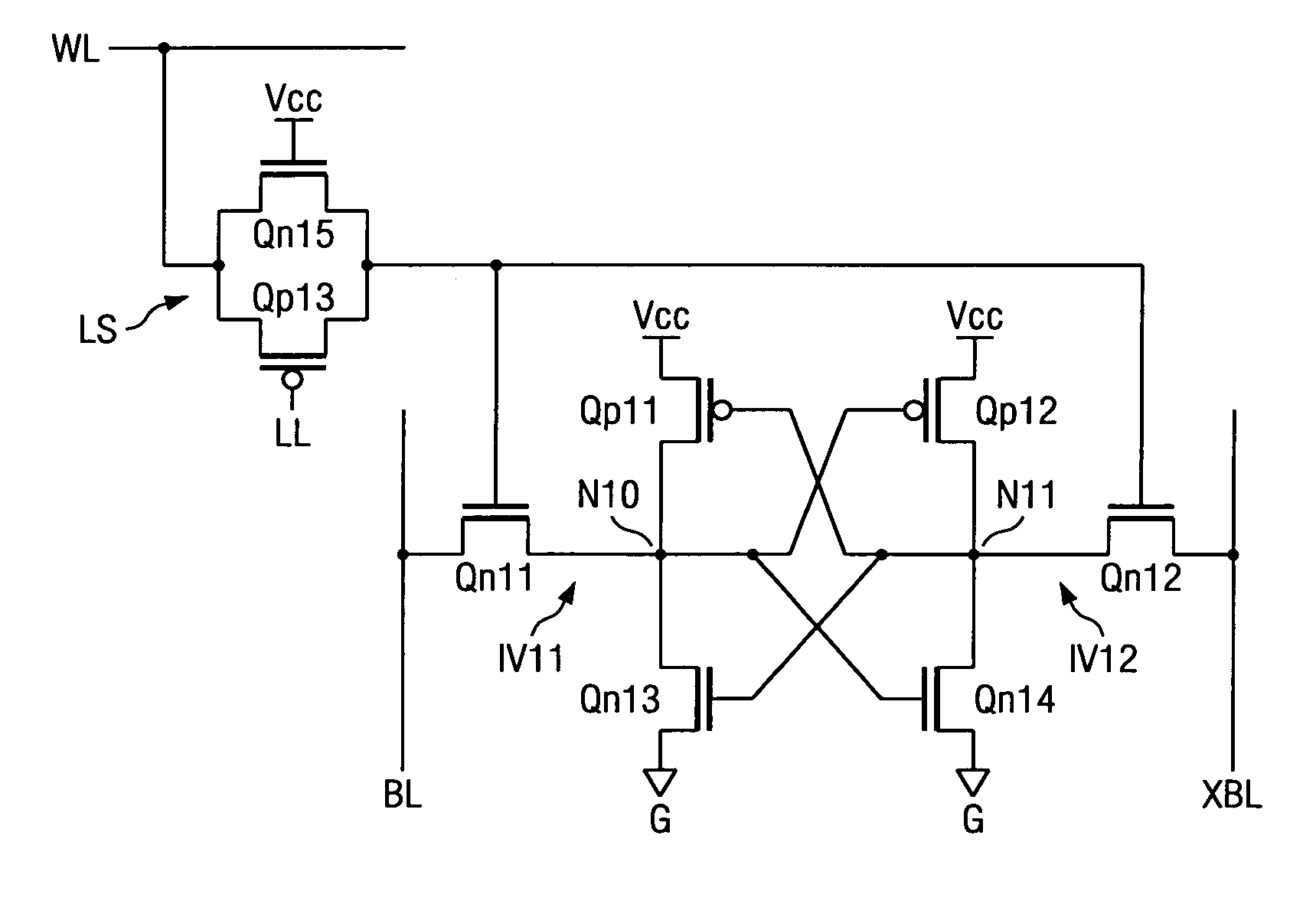
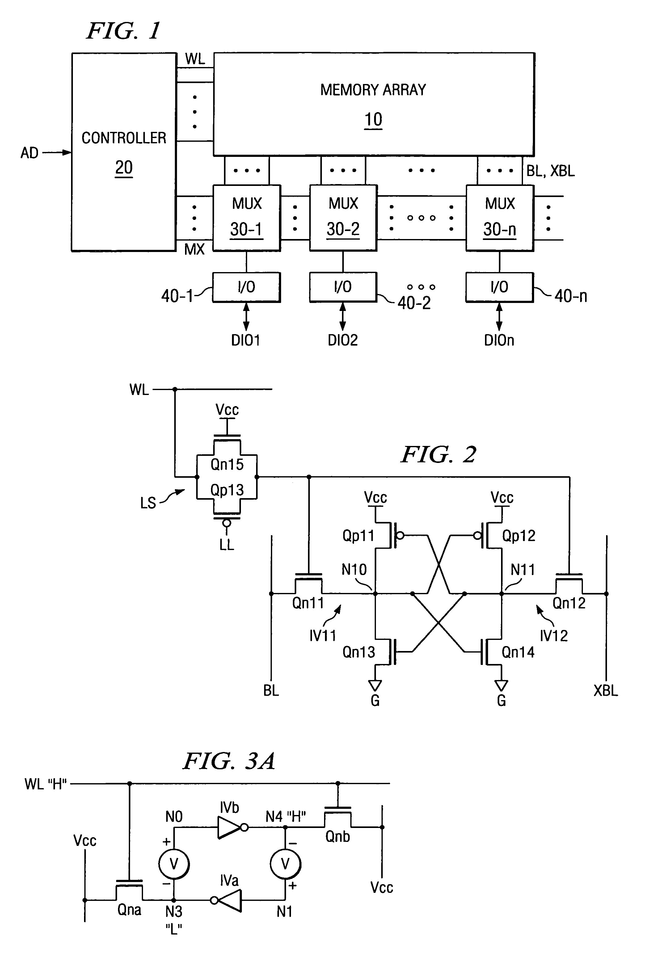
[0046]FIG. 1 is a diagram illustrating an example of the constitution of the SRAM device of Embodiment 1 of the present invention. The SRAM device shown in FIG. 1 comprises memory array 10, controller 20, column selecting circuits 30-1 to 30-n (where n is a natural number), and input / output circuits 40-1 to 40-n. Controller 20 shows an embodiment of the controller of the present invention. Memory array 10 contains plural memory cells arranged in an array. The memory cells that are arranged side by side in the same row are connected to the common word line WL, and the memory cells that are arranged side by side in the same column are connected to the common bit line pair BL, XBL. Also, among said plural memory cells, the memory cells arranged side by side in the same column are connected to common level control line LL. Level signal line LL is a signal line that transmits the control signal for level conversion (level control signal) to be explained below.

[0047]Among plural word line...

embodiment 2

[0071]Embodiment 2 of the present invention will be explained below.

[0072]FIG. 8 is a diagram illustrating an example of the constitution of the SRAM device in Embodiment 2 of the present invention. The SRAM device shown in FIG. 8 has main array 11, write controller 21, read controller 22, column selecting circuits 31-1 to 31-n, 32-1 to 32-n, input circuits 41-1 to 41-n, and output circuits 42-1 to 42-n. Write controller 21 is an embodiment of the first controller of the present invention. Read controller 22 is an embodiment of the second controller of the present invention. Memory array 11 also has plural memory cells arranged in an array like memory array 10. Of these plural memory cells, the memory cells arranged side by side in the same row are connected to the common write word line WWL and read word line pair RWL, XRWL, and at the same time, the memory cells arranged side by side in the same column are connected to the common write bit line pair WBL, XWBL and read bit line RBL...

embodiment 3

[0091]Embodiment 3 will be explained below.

[0092]FIG. 12 is a diagram illustrating an example of the constitution of the SRAM device pertaining to Embodiment 3. For the SRAM device shown in FIG. 12, memory array 11 in the SRAM device shown in FIG. 8 is replaced with memory array 11A (to be explained below), and at the same time, channel wiring portions 51 and 52 are arranged between memory array 11A and column selecting circuits 31-1 to 31-n, 32-1 to 32-n.

[0093]FIG. 13 is a diagram illustrating an example of the constitution of memory cells MC1, MC2, . . . and level conversion circuits LS1, LS2, . . . contained in said memory array 11A. As shown in FIG. 13, memory cells MC1, MC2, . . . have the same constitution as that of the memory cell shown in FIG. 9 excluding level conversion circuit LS (that is, Qn11, Qn12, Qn17, Qp15, IV11–IV13). Although not shown in the figure, the constitution is the same as said memory array 11 with respect to the connection of write bit line pair WBL, XW...


PUM


Abstract

The objective of this invention is to provide a static memory cell and an SRAM device that can improve the write margin while preventing degradation of the static noise margin. By turning on / off transistor Qp13, it is possible to control the drop in voltage due to the threshold voltage of transistor Qn15. For example, in read mode, when it is necessary to hold the stored data while setting word line WL to the high level, transistor Qp13 is turned off; the drivability of transistor pair Qn11, Qn12 is decreased, thereby increasing the static margin. In the case of rewriting the stored data, transistor Qp13 is turned on; the drivability of transistor pair Qn11, Qn12 is increased, thereby increasing the write margin. As a result, it is possible to improve the performance of both the static noise margin and the write margin.

Description

FIELD OF THE INVENTION[0001]The present invention pertains to a memory cell and semiconductor memory device. In particular, the present invention pertains to a static memory cell and SRAM device with improved static noise margin, write margin and other properties.BACKGROUND OF THE INVENTION[0002]FIG. 15 is a diagram illustrating an example of the constitution of the memory cell in a general 1-port SRAM (static random-access memory). The memory cell shown in FIG. 15 has six transistors (n-type MOS transistors Qn1–Qn4, p-type MOS transistors Qp1, Qp2). Among said transistors, p-type MOS transistor Qp1 and n-type MOS transistor Qn3 form inverter circuit IV1, and p-type MOS transistor Qp2 and n-type MOS transistor Qn4 form inverter circuit IV2. The inputs and outputs of inverter circuits IV1 and IV2 are connected in the form of a ring, and the signal levels of connecting nodes N0 and N1 are held at complementary levels. That is, one node is held at the high level, while the other node i...

Claims


Application Information

Patent Timeline
Patent Type & Authority Patents(United States)
IPC IPC(8): G11C11/00G11C5/14G11C8/08G11C11/41G11C11/412
CPCG11C11/412G11C8/08
Inventor MATSUZAWA, TAKAHIROSAITOH, YORITAKAHIRA, MASAYUKI
Owner TEXAS INSTR INC
Why Eureka
Try Eureka