Semiconductor memory device

Inactive Publication Date: 2005-12-01
PS4 LUXCO SARL
View PDF8 Cites 7 Cited by
  • Summary
  • Abstract
  • Description
  • Claims
  • Application Information

AI Technical Summary

Benefits of technology

[0013] On the other hand, in the read operation, the speed to read electric charges of memory cell capacitor into the bit line strongly depends on current drivability of memory cell transistor. As drivability lowers, the time for reading memory cell data to the bit line increases, and access time and cycle time become longer.
[0014] Consequently, in order to achieve high-speed access and short cycle time, current drivability of memory cell transistor must be improved. To improve current drivability of memory transistor, there are methods to increase the gate voltage as well as to increase the memory cell transistor size. However, increased gate voltage degrades reliability of miniaturized transistors, and increased chip area results because the scale of the charge pump circuit increases.
[0018] That is, the semiconductor memory device according to the present invention has a configuration in which two memory cell transistors comprising a first transistor and a second transistor are connected in parallel across the bit line and capacitor element. Using these two memory cell transistors for reading / writing in and from a capacitor element enables the improvement of current drivability.
[0023] By this kind of configuration, for the capacitor element as described above, a configuration in which two memory cell transistors are connected in parallel can be achieved as a memory cell array configuration. And this memory array configuration is best-suited for increased integration. In addition, by making the shape of the active region and bit line, for example, triangular wave shaped which is continued in the bit line direction, the configuration of arrangement that can secure the capacitor area can be secured.

Problems solved by technology

On the other hand, because with respect to the memory cell transistor, from the viewpoint of leakage prevention of capacitor accumulated electric charges, the threshold voltage cannot be lowered, the word line swing voltage cannot be lowered and reduction of gate oxide thickness cannot be undertaken, even if miniaturization advances.
Consequently, as miniaturization advances, current drivability lowers.
As a result, when the specified electric charge amount is written in the memory cell capacitor, or accumulated electric charges are read from the memory cell capacitor, problems of increased writing time and increased reading time occur.

Method used


Image

  • Semiconductor memory device
  • Semiconductor memory device
  • Semiconductor memory device

Examples


embodiment 1

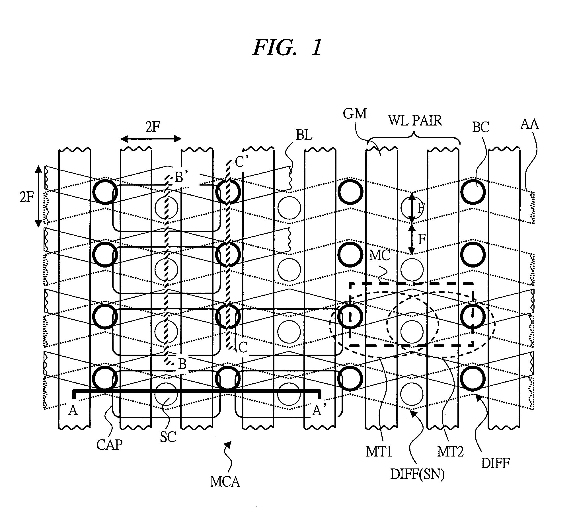
[0059]FIG. 1 is a layout drawing showing one example of the memory cell layout in a semiconductor memory device according to embodiment 1 of the present invention. FIG. 2 is an equivalent circuit diagram that corresponds to the memory cell layout of FIG. 1.

[0060] As illustrated in FIG. 2, the semiconductor memory device according to embodiment 1 of the present invention has a memory cell MC at a desired intersection between a word line WL and a bit line BL in a memory cell array MCA, and one memory cell MC comprises two memory cell transistors MT1, MT2 and one capacitor Cs to store information as electric charges. In the memory cell MC, to a storage node SN (first node), one ends of source terminal / drain terminal of two memory cell transistors MT1, MT2 and one end of capacitor Cs are connected in common, and to bit line BL1, the other ends (second node) of memory cell transistors MT1, MT2 are independently connected, respectively.

[0061] Let the wiring pitch of word line WL be 2F (...

embodiment 2

[0090]FIG. 3 is a layout drawing showing one example of the memory cell layout in a semiconductor memory device according to embodiment 2 of the present invention. The memory cell layout shown in FIG. 3 differs from FIG. 1 described above and is characterized in that the bit line and wiring patterns of the diffusion layer row are wired to achieve waveforms of 8F cycle.

[0091] The bit line contact BC is disposed at the portion where the bit line BL and the diffusion layer row (active region AA) intersect, and the storage node contact SC is disposed at the position where the bit line BL and the diffusion layer row do not overlap in the perpendicular line but is disposed at the position shifted just by F. The storage node contact SC of the memory cell MC connected to the bit line BL is disposed alternately top and bottom with respect to the bit line BL. Because this arrangement can make the wave-form cycle of the bit line BL and diffusion layer row become 8F as described above as well ...

embodiment 3

[0097]FIG. 4 is a layout drawing showing one example of the memory cell layout in a semiconductor memory device according to embodiment 3 of the present invention. The memory cell layout shown in FIG. 4 differs from cases of embodiments 1, 2 and bit lines and diffusion layer row are disposed perfectly parallel in the vertical direction, and is a suitable layout in which the capacitor is formed below the bit line wiring layer.

[0098] According to this kind of layout, since the bit lines and diffusion layer row are disposed completely in parallel in the vertical direction, processing and formation of bit lines and diffusion layer row become easy. In addition, because same as the cases of embodiments 1, 2 described above, the width of the diffusion layer region which is the gate width of memory cell transistor becomes F, the total gate width of the memory cell transistors connected between one memory cell capacitor and the bit line becomes 2F. The area of memory cell MC in this event i...


PUM


Abstract

A semiconductor memory device that can achieve high-speed operation or that is highly integrated and simultaneously can achieve high-speed operation is provided. Transistors are disposed on both sides of diffusion layer regions to which capacitor for storing information is connected and other diffusion layer region of each transistor is connected to the same bit line. When access to a memory cell is made, two transistors are activated and the information is read. When writing operation to the memory cell is carried out, two transistors are used and electric charges are written to the capacitor.

Description

CROSS-REFERENCE TO RELATED APPLICATION [0001] The present application claims priority from Japanese Patent Application No. JP 2004-154753 filed on May 25, 2004, the content of which is hereby incorporated by reference into this application. TECHNICAL FIELD OF THE INVENTION [0002] The present invention relates to a dynamic semiconductor memory device and specifically to a technique which is effective to be applied for configuration of the storage element portion of the device. BACKGROUND OF THE INVENTION [0003] For example, in the dynamic random access memory (DRAM), information is stored by accumulating electric charges in a capacitor via memory-cell transistor. In DRAM, the area the memory cell occupies decreases as integration increases and miniaturization advances. [0004] As a conventional DRAM memory cell configuration, for example, the following one can be mentioned set forth in: Jong-Wan Jung and seven others: A fully working 0.14 μm DRAM technology with polymetal (W / WNx / Poly-...

Claims


Application Information

Patent Timeline
IPC IPC(8): G11C11/24H01L27/108G11C11/405G11C11/4097H01L21/8242H01L27/02
CPCG11C11/405G11C11/4097H01L27/10873H01L27/108H01L27/10814H01L27/0207H10B12/315H10B12/05H10B12/00G11C11/401H01L21/108G11C11/407
Inventor TAKEMURA, RIICHIROAKIYAMA, SATORUHANZAWA, SATORUSEKIGUCHI, TOMONORIKAJIGAYA, KAZUHIKO
Owner PS4 LUXCO SARL
Why Eureka
Try Eureka