Nonvolatile memory cell operating by increasing order in polycrystalline semiconductor material

Inactive Publication Date: 2005-10-13
SANDISK TECH LLC
View PDF63 Cites 365 Cited by
  • Summary
  • Abstract
  • Description
  • Claims
  • Application Information

AI Technical Summary

Benefits of technology

[0009] Yet another aspect of the invention provides for a method for forming and programming a nonvolatile memory cell, the method comprising: forming a first conductor; forming a second conductor; depositing and doping semiconductor material to form a semiconductor junction diode, the semiconductor junction diode disposed between the first and second conductors; crystallizing the semiconductor material such that the semiconductor junction diode is polycrystalline, wherein, during the crystallizing step, the semiconductor

Problems solved by technology

When a sufficiently large voltage is applied between the conductors, however, the dielectric antifuse layer suffers dielectric breakdown and ruptures, and a permanent conductive path is formed through the dielectric antifuse layer.
If the dielectric antifuse layer is too thin, leakage current can be a severe problem.
Disturb can also be a problem: Every time the memory cell is read, the dielectric antifuse l

Method used


Image

  • Nonvolatile memory cell operating by increasing order in polycrystalline semiconductor material
  • Nonvolatile memory cell operating by increasing order in polycrystalline semiconductor material
  • Nonvolatile memory cell operating by increasing order in polycrystalline semiconductor material

Examples


Embodiment Construction

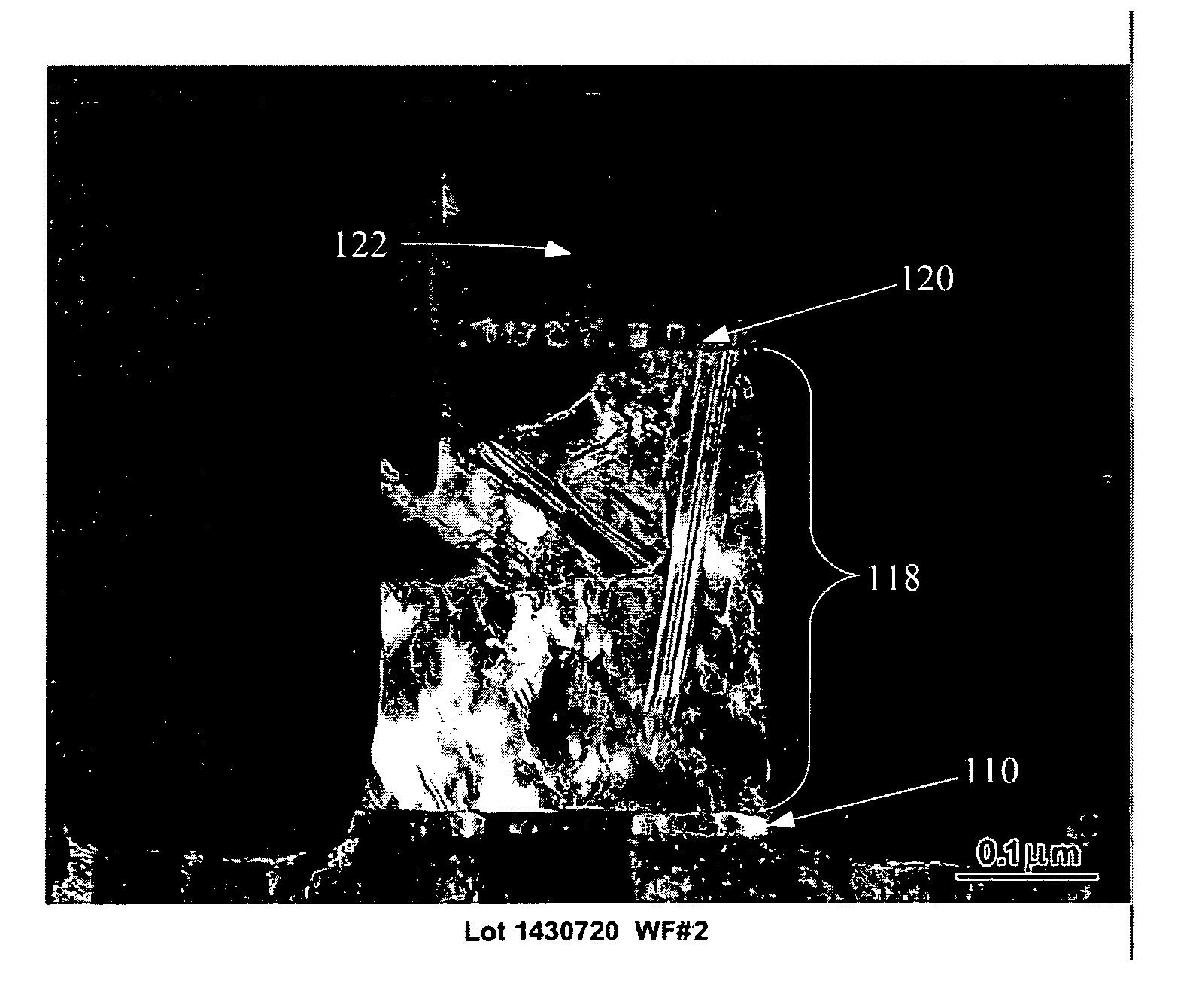
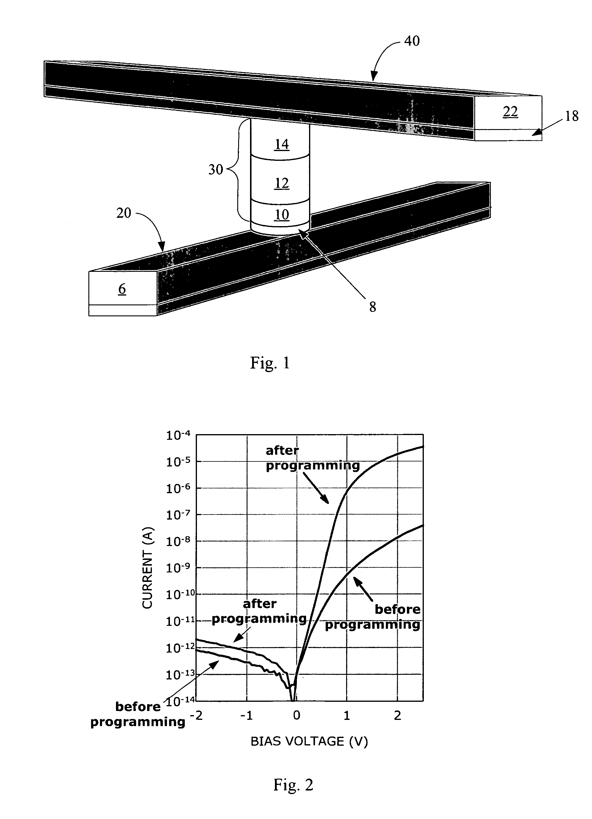
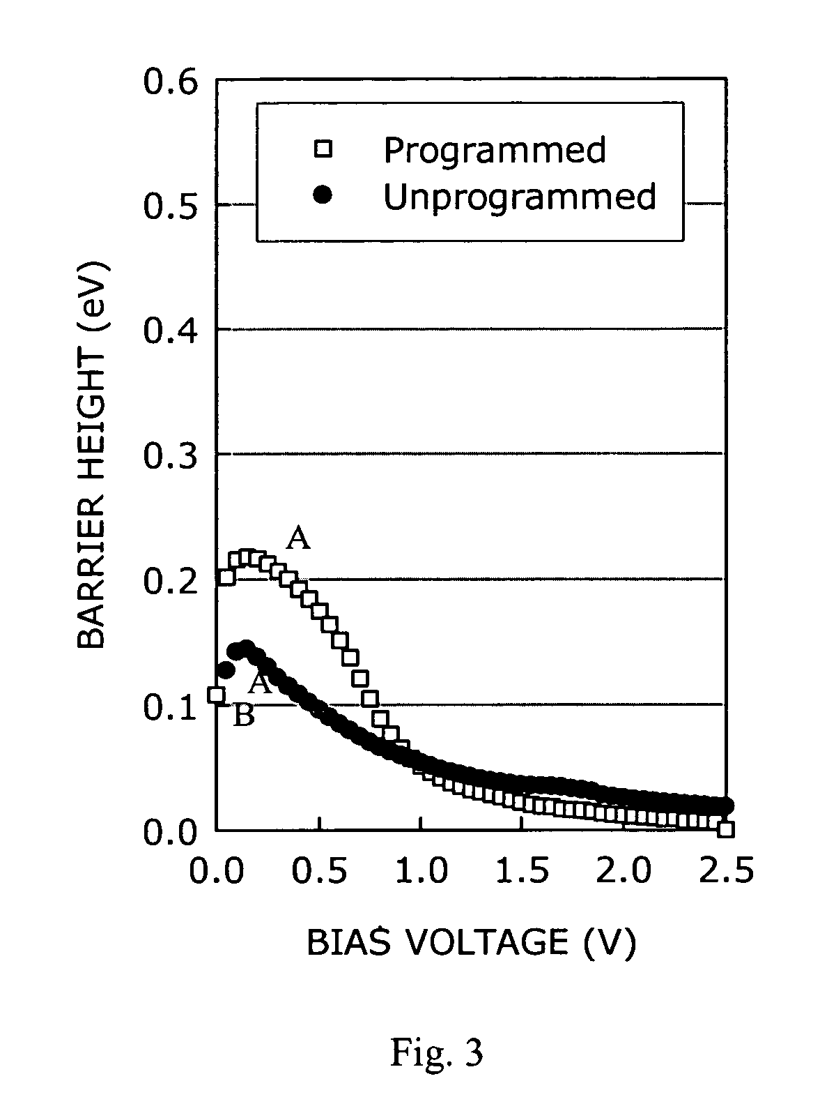
[0006] The present invention is defined by the following claims, and nothing in this section should be taken as a limitation on those claims. In general, the invention is directed to a nonvolatile memory cell comprising a diode, the memory state stored in the state of the diode.

[0007] A first aspect of the invention provides for a nonvolatile memory cell comprising: a first conductor; a diode comprising amorphous or polycrystalline semiconductor material; and a second conductor, the semiconductor diode disposed between the first conductor and the second conductor, wherein before application of a programming voltage the diode has a first maximum barrier height, and after application of the programming voltage the diode has a second maximum barrier height, the second maximum barrier height at least 1.5 times the first maximum barrier height.

[0008] Another aspect of the invention provides for a nonvolatile memory cell comprising: a first conductor; a second conductor; and a polycryst...


PUM


Abstract

A nonvolatile memory cell is described, the memory cell comprising a semiconductor diode. The semiconductor material making up the diode is formed with significant defect density, and allows very low current flow at a typical read voltage. Application of a programming voltage permanently changes the nature of the semiconductor material, resulting in an improved diode. The programmed diode allows much higher current flow, in some embodiments one, two or three orders of magnitude higher, at the same read voltage. The difference in current allows a programmed memory cell to be distinguished from an unprogrammed memory cell. Fabrication techniques to generate an advantageous unprogrammed defect density are described. The memory cell of the present invention can be formed in a monolithic three dimensional memory array, having multiple stacked memory levels formed above a single substrate.

Description

RELATED APPLICATIONS [0001] This application is a continuation-in-part of Herner et al., U.S. patent application Ser. No. 10 / 955,549, “Nonvolatile Memory Cell Without a Dielectric Antifuse Having High- and Low-Impedance States,” filed Sep. 29, 2004 and hereinafter the '549 application; itself a continuation-in-part of Herner et al., U.S. patent application Ser. No. 10 / 855,784, “An Improved Method for Making High-Density Nonvolatile Memory,” filed May 26, 2004; which is a continuation of Herner et al., U.S. patent application Ser. No. 10 / 326,470, “An Improved Method for Making High-Density Nonvolatile Memory,” filed Dec. 19, 2002 (since abandoned) and hereinafter the '470 application, all assigned to the assignee of the present invention and hereby incorporated by reference in their entirety.BACKGROUND OF THE INVENTION [0002] The invention relates to a nonvolatile one-time-programmable memory cell. [0003] Prior art nonvolatile memories, such as Johnson et al., U.S. Pat. No. 6,034,882...

Claims


Application Information

Patent Timeline
IPC IPC(8): G11C7/00G11C11/39G11C17/06G11C17/16G11C29/00H01L21/336H01L21/82H01L27/24H01L29/73H01L45/00
CPCG11C5/02G11C11/39G11C11/36G11C17/16H01L27/1021G11C17/06H01L21/82H01L29/66477H10B63/20H10N70/20
Inventor HERNER, S. BRADBANDYOPADHYAY, ABHIJIT
Owner SANDISK TECH LLC
Why Eureka
Try Eureka