Organic electroluminescent device
a technology of electroluminescent devices and electroluminescent lamps, which is applied in the direction of discharge tubes luminescnet screens, discharge tubes/lamp details, electric discharge lamps, etc., can solve the problems of significant increase in driving voltage, and achieve low driving voltage and high efficiency.
- Summary
- Abstract
- Description
- Claims
- Application Information
AI Technical Summary
Benefits of technology
Problems solved by technology
Method used
Image
Examples
example 1
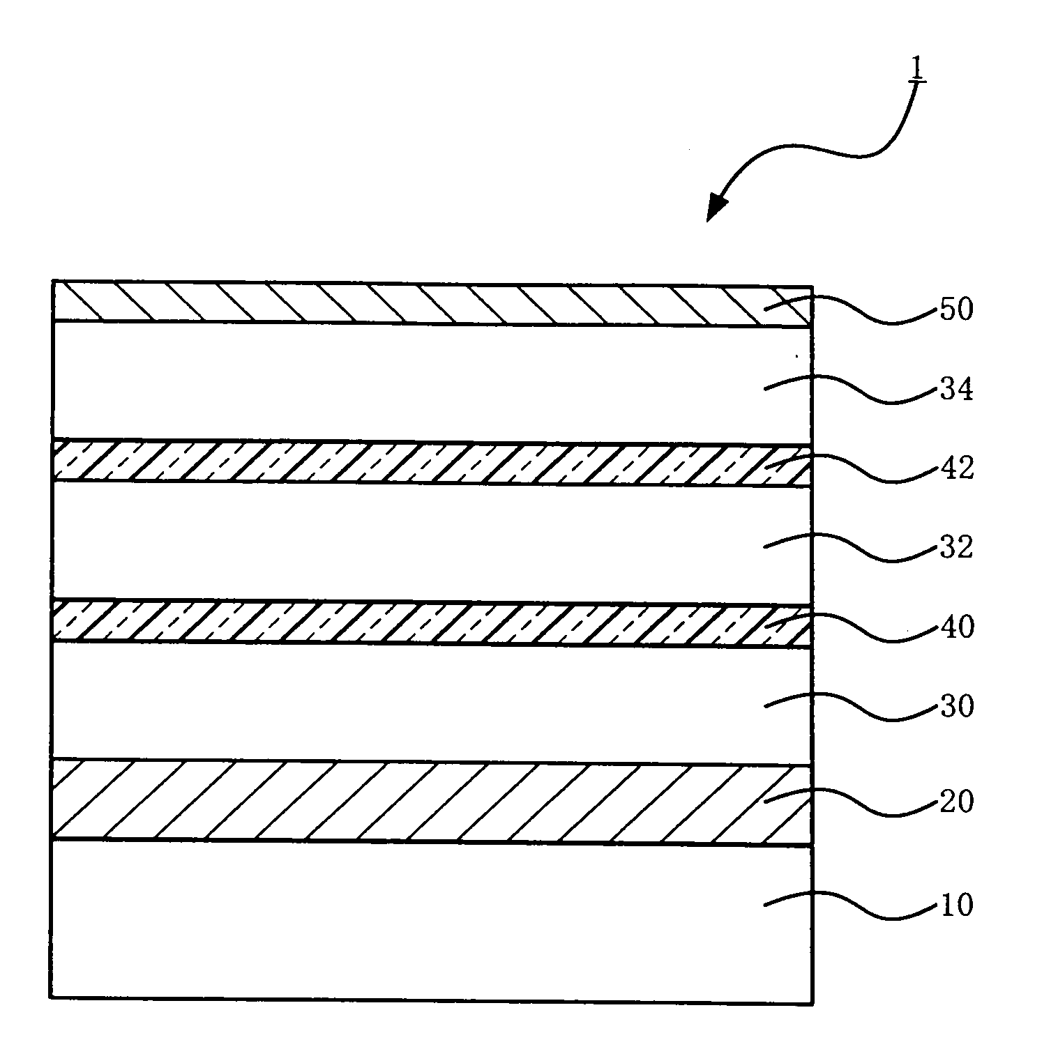
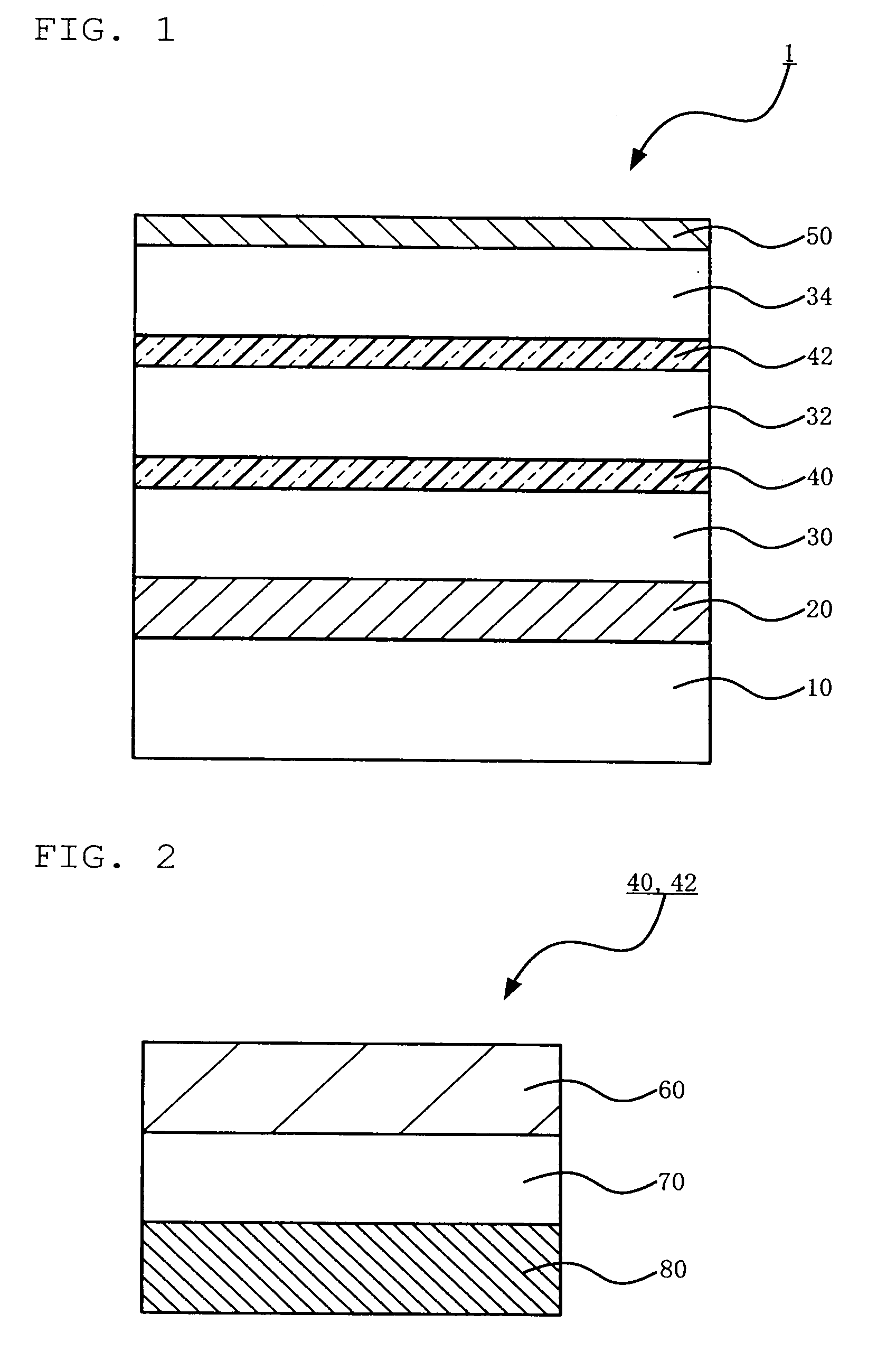
[0171]An organic EL device having the following device configuration as the configuration of the anode / the first organic emitting layer / the intermediate connection layer / the second organic emitting layer / the cathode was fabricated. ITO(130) / Ac1(40) / HT1 (40) / BH:BD1(40; 40:2) / ET1(20) / LiF(1.0) / A c1(40) / HT1(40) / BH:BD1(40; 40:2) / ET1(20) / LiF(1.0) / Al(150)
[0172]On a 0.7 mm-thick glass substrate, an ITO film was formed into a thickness of 130 nm by sputtering. Thereafter, the substrate was subjected to ultrasonic cleaning in isopropyl alcohol for 5 minutes, and cleaned with ultraviolet ozone for 30 minutes. Then, the substrate with the ITO electrode was mounted on a substrate holder in a vacuum vapor deposition apparatus.
[0173]Ac1 as a material for the hole-injecting layer of the first organic emitting layer and as a material for the acceptor layer of the intermediate connection layer, HT1 as a material for the hole-transporting layer of the first and second organic emitting layers, BH as a ...
example 2
[0176]An organic EL device was fabricated in the same manner as in Example 1, except that ET2 was used instead of ET1 in the electron-transporting material layer of the intermediate connection layer and in the electron-transporting layer of the second organic emitting layer.
example 3
[0177]An organic EL device was fabricated in the same manner as in Example 1, except that ET3 was used instead of ET1 in the electron-transporting material layer of the intermediate connection layer and in the electron-transporting layer of the second organic emitting layer.
PUM
 Abstract
Description
Claims
Application Information


