Memory device and method of operating same

a memory device and memory technology, applied in semiconductor devices, digital storage, instruments, etc., can solve the problems of slow reading and programming, consuming a relatively large amount of power, and increasing the difficulty of cell scaling down to smaller sizes

Inactive Publication Date: 2005-08-30
SILICON STORAGE TECHNOLOGY
View PDF17 Cites 359 Cited by
  • Summary
  • Abstract
  • Description
  • Claims
  • Application Information

AI Technical Summary

Problems solved by technology

However, EEPROM memory cells are getting more difficult to scale down to smaller sizes, are relatively slow to read and program, and can consume a relatively large amount of power.
The disadvantages of this cell array configuration are that an isolation device needs to be formed for each memory cell.
Further, because the memory device supplies a known voltage to the memory and reference cells, and then measures current therethrough, and any variation in resistance among the isolation devices will cause variations in the measured currents that are not attributable to the programmed resistivity of the memory cells themselves.
Leakage current through the isolation devices can also be problematic.

Method used


Image

  • Memory device and method of operating same
  • Memory device and method of operating same
  • Memory device and method of operating same

Examples


Embodiment Construction

[0027]The present invention is an improved configuration and interconnection of an array of programmable memory material cells, as well as an improved method of programming and reading such cells.

[0028]Individual Memory Cells

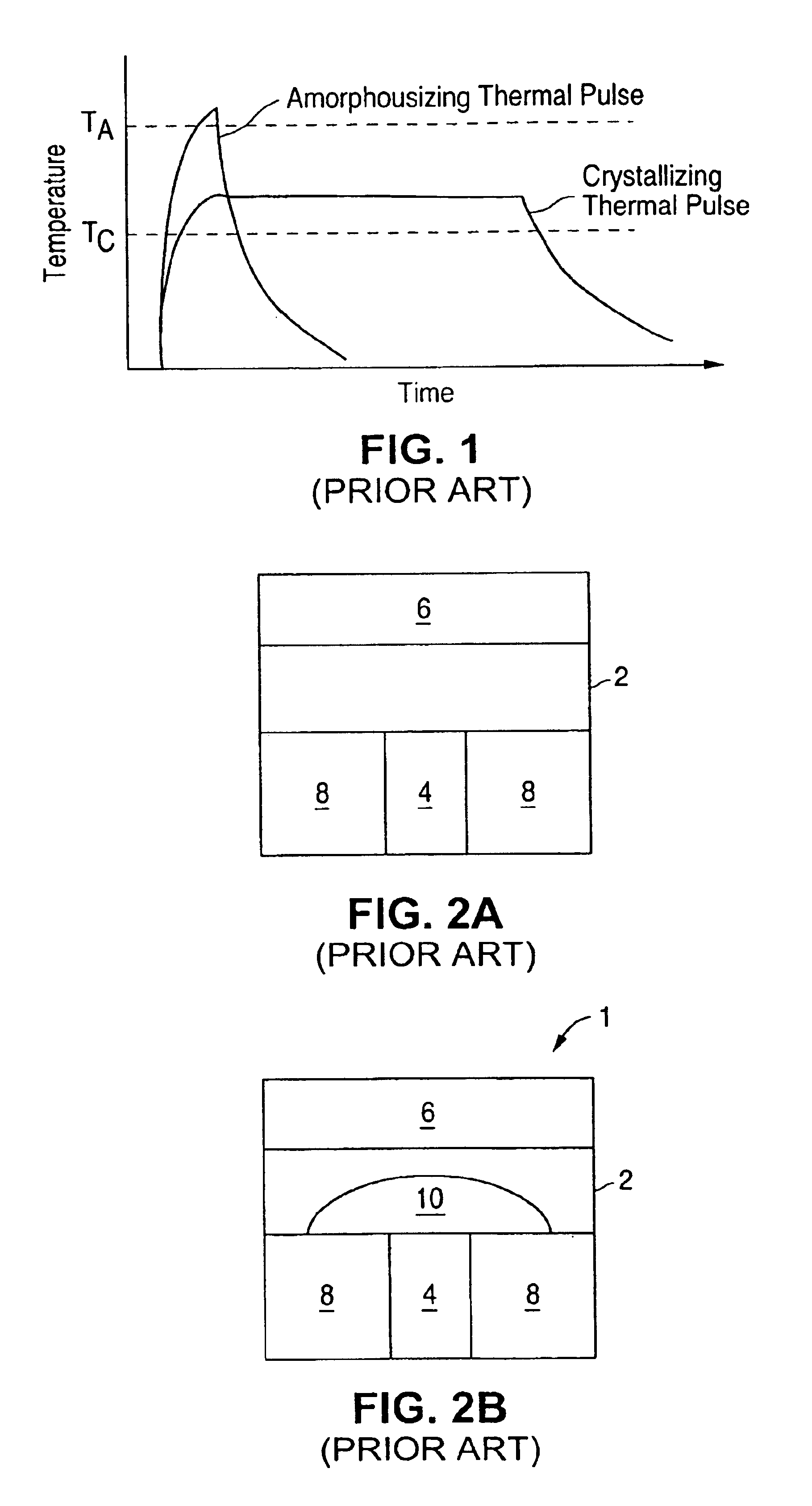
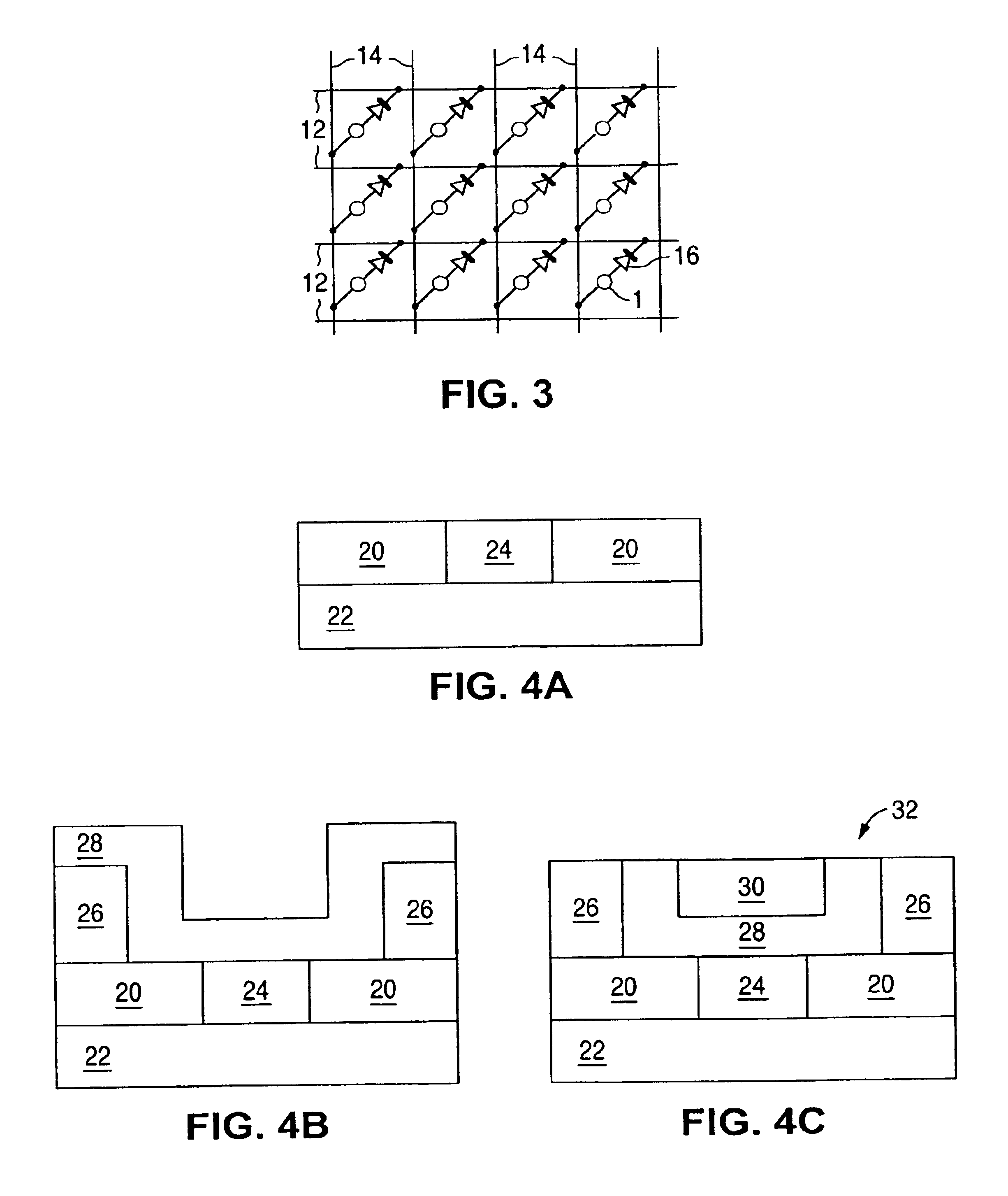
[0029]The individual memory cells used in the memory cell array of the present invention can be of many types that utilize phase change memory materials. FIGS. 4A to 4C illustrate a method of forming a phase change material memory cell used with the array of the present invention. The method begins by forming a layer 20 of insulation material (e.g. one or more layers of silicon dioxide—“oxide”, silicon nitride—“nitride”, ILD, etc.) over a silicon substrate 22 using a conventional deposition process. A (first) contact hole is formed in the insulation material 20 using a conventional lithographic etch process, which is then filled with a conductive material (e.g. tungsten, titanium-tungsten, etc.) by material deposition followed by a CMP (chemical-mechanical polis...


PUM


Abstract

An array of phase changing memory cells that includes a current source, a voltage sensor, a plurality of conductive bit lines electrically connected to the current source, a plurality of conductive word lines each electrically connected to a ground plane via a first resistor and to the voltage sensor, and a plurality of memory cells. Each memory cell is connected between one of the bit lines and one of the word lines and includes phase change memory material. One of the memory cells is selected by turning on switches just on the bit line and word line connected thereto, or by turning a switch connected in series between the corresponding bit and word lines, where the read current flows through the selected memory cell and the voltage sensor measures a voltage drop across the selected memory cell.

Description

FIELD OF THE INVENTION[0001]The present invention relates to phase change memory devices, and more particularly to an array of phase change memory devices.BACKGROUND OF THE INVENTION[0002]There are many types of computer memory technologies that are presently used to store computer programs and data, including dynamic random access memory (DRAM), static random access memory (SRAM), erasable programmable read-only memory (EPROM), and electrically erasable programmable read only memory (EEPROM), etc. Some memory technologies require electrical power to maintain the stored data (i.e. volatile memory), while others do not (i.e. non-volatile memory). Memory technologies can be read only, write once only, or repeatedly read / write.[0003]There is an increasing demand for repeatedly read / write, non-volatile memory. The primary non-volatile memory technology presently used is EEPROM, which utilizes floating gate field effect transistor devices each holding a charge on an insulated “floating g...

Claims


Application Information

Patent Timeline
Patent Type & Authority Patents(United States)
IPC IPC(8): G11C11/00G11C16/02H01L27/24
CPCG11C13/0004G11C13/004G11C13/0069H01L45/06H01L45/1233H01L45/126H01L45/1273H01L45/144H01L45/1666H01L27/2454H01L27/2481G11C2013/0054G11C2013/0078G11C2213/72G11C2213/77G11C2213/79H10B63/34H10B63/84H10N70/231H10N70/8413H10N70/8418H10N70/826H10N70/8828H10N70/061
Inventor CHEN, BOMY
Owner SILICON STORAGE TECHNOLOGY
Why Eureka
Try Eureka