Method for implementation of a low noise, high accuracy current mirror for audio applications

a high-accuracy, mirror circuit technology, applied in the direction of digital-analog converters, instruments, transmission systems, etc., can solve the problems of residual error current and added stress, and achieve the effect of accurate matching

Inactive Publication Date: 2006-08-15
DIALOG SEMICONDUCTOR GMBH
View PDF14 Cites 1 Cited by
  • Summary
  • Abstract
  • Description
  • Claims
  • Application Information

AI Technical Summary

Benefits of technology

[0006]It is an objective of the present invention to provide a current mirror load operating in conjunction with a DAC that provides an accurate output current that is accurately matched to the current mirror input current.
[0008]It is further an objective of the present invention to provide a current mirror circuit that produces a high current output, which matches a high current input with a high level of accuracy.
[0013]When there is no digital input signal to the DAC, it is important that the output of the amplifier is at it's quiescent bias point, which in turn does not put undue stress on the speaker device connected to the output of the amplifier. Slight differences in the output current of the current mirror circuit from the input current will cause a substantial error signal at the output of the amplifier, when connected in a high gain configuration, and when the digital input signal to the DAC corresponds to the zero level code. This amplified error signal in turn places a stress on the audio speakers.
[0014]In the present invention the error signal problem is substantially reduced or eliminated by accurately matching the high output current of the current mirror circuit to the high input current so that a zero audio signal is produced when the code input to the DAC corresponds to a zero level. To accomplish this, the high current circuitry of the current mirror is formed in a symmetrical array of N-channel transistor devices. The array of N-channel transistor devices is divided into two groups, a first group for handling input current from the DAC and a second group for providing an output current of the current mirror circuit. The two groups of N-channel transistor devices are distributed and intermingled within the array of N-channel transistor devices in a checkerboard fashion. The distributed checkerboard fashion allows the composite of all transistor devices in each group to smooth, or average out process variations in the transistor devices. All of the N-channel transistor devices in the first group are connected in parallel, wherein all gates are connected together, all drains are connected together and all sources are connected together. In like manner all N-channel transistor devices in the second group are connected in parallel, wherein all gates are connected together, all drains are connected together and all sources are connected together.
[0015]A symmetrical source voltage distribution network is positioned over the symmetrical array of N-channel transistors and is connected to all the sources in the array of N-channel transistors such that the same voltage value is connected to each source. A metallization carrying the source voltage to the array of N-channel transistor devices is connected to the symmetrical source voltage distribution network at a central point in the network, thus allowing the distribution network to supply each source of the N-channel transistors of the two groups of N-channel transistors with the same source voltage. The metallization carrying the source voltage to the source voltage distribution network and the source voltage distribution network are formed with wide high current carrying metallization providing sufficiently low impedance.
[0016]The input current path to the current mirror from the DAC and the output current path from the current mirror are formed with wide high current carrying metallization to have equal impedance so that the same voltage drops occur in each path. A plurality of vias between metallization on different wiring layers of the semiconductor device are used to further minimize resistance of the high current carrying paths and to reduce effects of temperature on the resistance of a particular high current path. This is important because the matching of vias is often uncontrolled or poorly controlled. The difference between the two currents is sensitive to variations in the high current output of the current mirror circuit. The output of the current mirror is centered around a reference voltage so that a negative digital input to the DAC can be coupled to the amplifier through the analog circuitry as a signal below the reference voltage. When there is no digital input signal to the DAC, the reference voltage is coupled to the amplifier and no analog error signal is coupled to the speaker mechanism. The techniques of the present invention provide a matching of the mirror current to the input current to which is produced an amplified accuracy at the amplifier greater than 0.01% when referred to the input signal level of the current mirror and herein called input referred accuracy.

Problems solved by technology

When the output from the current mirror circuit does not perfectly match the input current to the current mirror circuit from the DAC, a residual error current results.
This becomes a problem when there is no digital input signal and the error current is converted to a voltage, which is applied to the sound-producing device and places an added stress on the coils of the earphone or other sound producing devices driven by the subsequent audio circuitry.

Method used


Image

  • Method for implementation of a low noise, high accuracy current mirror for audio applications
  • Method for implementation of a low noise, high accuracy current mirror for audio applications
  • Method for implementation of a low noise, high accuracy current mirror for audio applications

Examples


Embodiment Construction

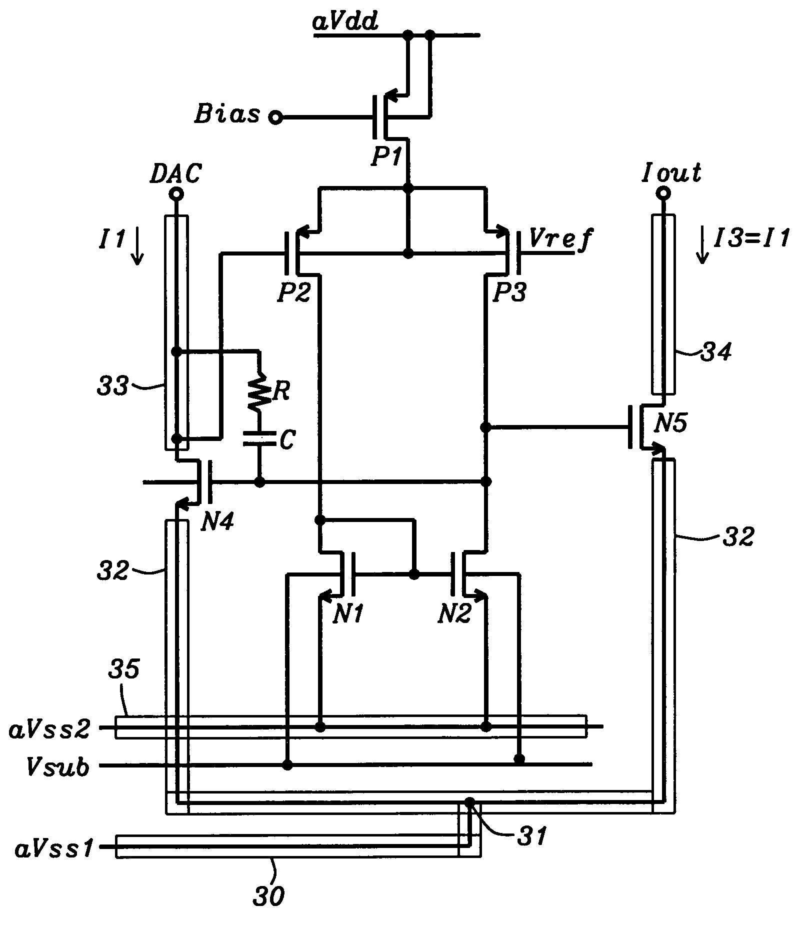
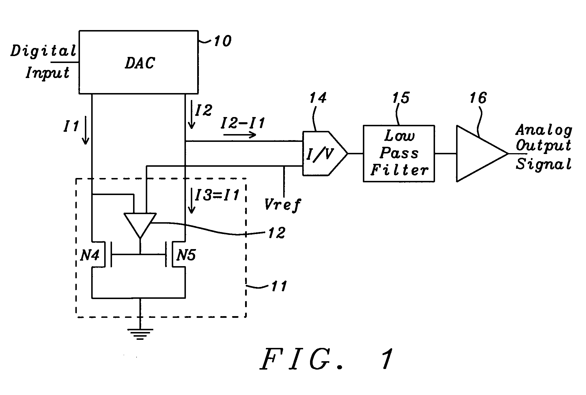
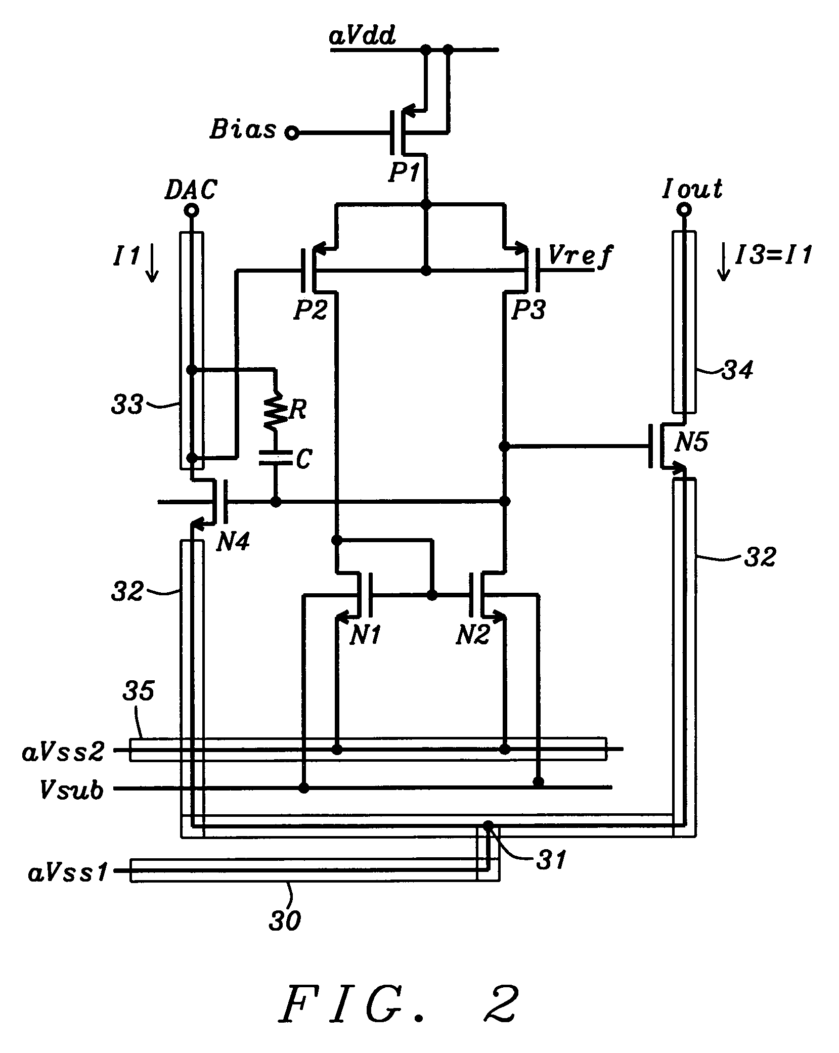
[0027]In FIG. 1 is shown the circuitry of the present invention to convert a digital signal to audio analog signal. A digital input signal is connected to a DAC 10, which is a current steering sigma delta DAC that produces two currents, I1 and I2 that are a function of the digital input, where I2 is approximately twice the magnitude of I1. Other DAC designs that produce similar currents are within the scope of this invention. The current I1 forms an input to the current mirror circuit 11. The current mirror circuit is symbolized by an amplifier 12, which drives the gates of two N-channel transistors, N4 and N5. The output current of the current mirror circuit is I3 where I3=I1. The amplifier 12 and a current to voltage converter 14 are connected to a reference voltage Vref around which the current, I2−I3=I2−I1, flows into the current to voltage converter. The currents I1, I2 and I3 are high currents, for example in the milliampere range but are not limited to this range. The referen...


PUM


Abstract

An accurate high current mirror circuit produces a mirrored current that matches an input current to produce an accuracy at the output of a subsequent stage of amplification of greater than 0.01%. A plurality of transistor devices are arranged in a symmetrical configuration and divided into two groups. The transistors in each of the two groups are connected in parallel to produce a high mirror current from a high input current. A distribution of a source voltage produces the same source voltage at each of the plurality of transistors. An input current metallization and a mirror current metallization are formed within the symmetrical configuration to have a same value of impedance. A plurality of P-channel transistors within the current mirror circuit control a voltage of a point on the input metallization to be the same as a reference voltage, thus causing the mirror current to be referenced around the reference voltage.

Description

BACKGROUND OF THE INVENTION[0001]1. Field of Invention[0002]The present invention relates to a current mirror circuit and more particularly a low noise and high accuracy current mirror circuit for audio applications.[0003]2. Description of Related Art[0004]In audio applications such as can be found in mobile phones producing an analog signal from a digital signal that can then be heard by the human ear requires a wide conversion range, i.e. twenty-four bits. This is often done with a current steering circuit where a sigma-delta DAC (digital to analog converter) with a low resolution DAC and a modulator drives a current mirror circuit. The current mirror circuit works in conjunction with the DAC to translate a digital code into a current centered around zero by taking the output from the current mirror circuit, whose input was driven by one output from the DAC and subtract it from the second output current from the DAC. When the output from the current mirror circuit does not perfect...

Claims


Application Information

Patent Timeline
Patent Type & Authority Patents(United States)
IPC IPC(8): H03M1/00
CPCG05F3/262
Inventor TESTER, DAVIDHAGUE, GARYMEDWED, JORG
Owner DIALOG SEMICONDUCTOR GMBH
Why Eureka
Try Eureka