Antenna device and wireless communication apparatus

a wireless communication and antenna technology, applied in the structure of radiating elements, elongated active elements, resonant antennas, etc., can solve the problems of significant degradation of antenna gain, degradation of antenna efficiency, and related antenna devices, so as to improve antenna efficiency and accurate matching

Active Publication Date: 2009-05-21
MURATA MFG CO LTD
View PDF12 Cites 73 Cited by
  • Summary
  • Abstract
  • Description
  • Claims
  • Application Information

AI Technical Summary

Benefits of technology

[0027]The disclosed antenna device solves the foregoing problems, and provides an antenna device capable of not only achieving multiple resonances and wideband characteristics but also achieving improvement of antenna efficiency and accurate matching at all resonant frequencies, and a wireless communication apparatus.

Problems solved by technology

However, the antenna devices of the related art described above have the following problems.
The antenna device 100 shown in FIG. 19 suffers from significant degradation of antenna gain.
In general, in compact antenna devices, the use of a lower resonant frequency decreases antenna gain, resulting in degradation of antenna efficiency.
In such a situation, loss due to the switching operation reduces antenna gain, resulting in further degradation of antenna efficiency.
The antenna device 200 shown in FIG. 20 also suffers from degradation of antenna efficiency.
Power consumption at the variable capacitance element 211 becomes large, resulting in great degradation of antenna efficiency.
In the antenna device 300 shown in FIG. 21, it is difficult to reduce the antenna size.
In the antenna device 300, further, it is difficult to match impedance between the feed unit side and the antenna side at all frequencies.
Therefore, unlike the antenna device shown in FIG. 20, the power consumed by the variable capacitance element is significantly small.
Further, the power consumed by the grounded variable capacitance element is significantly small.

Method used


Image

  • Antenna device and wireless communication apparatus
  • Antenna device and wireless communication apparatus
  • Antenna device and wireless communication apparatus

Examples


first embodiment

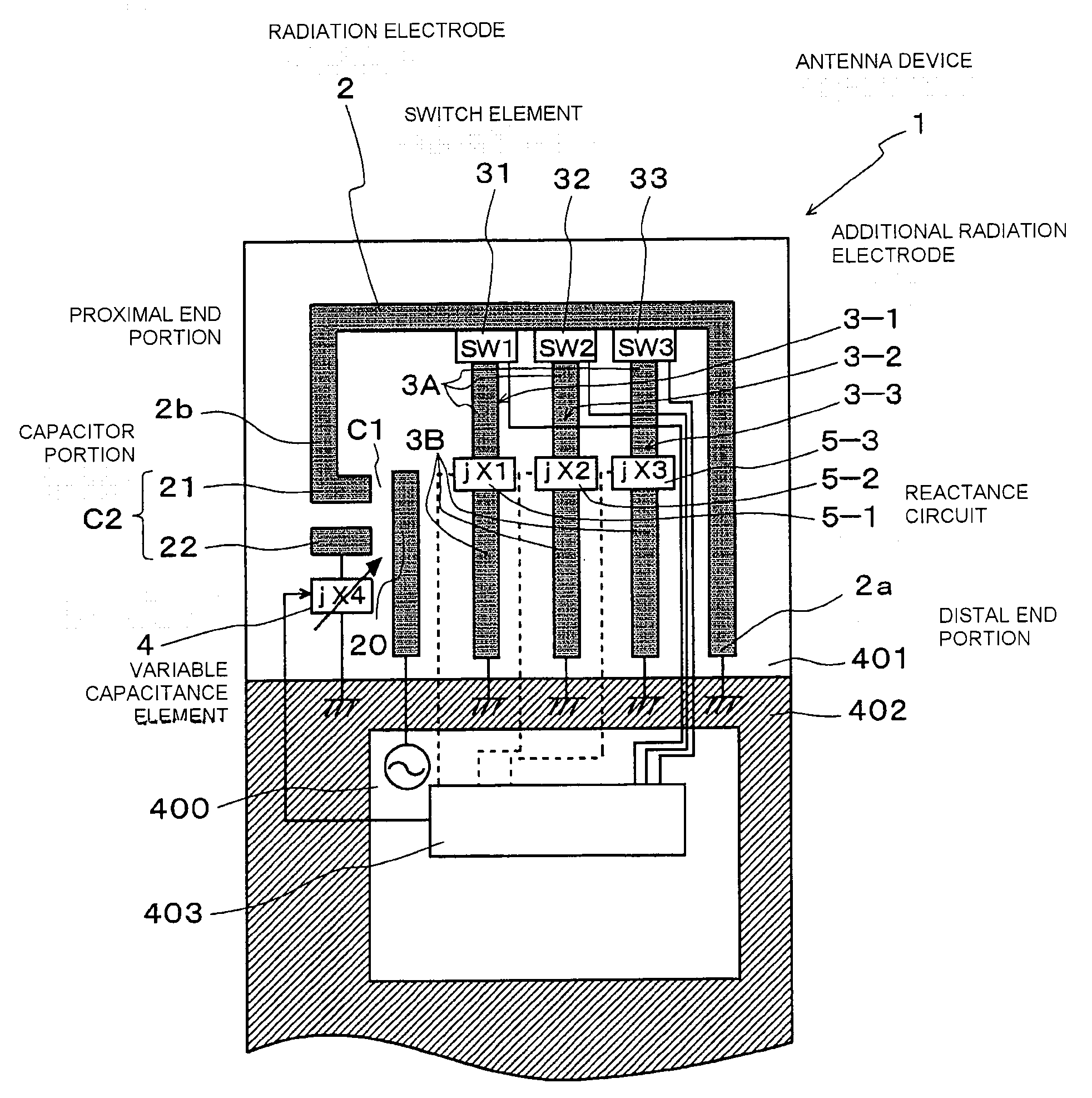
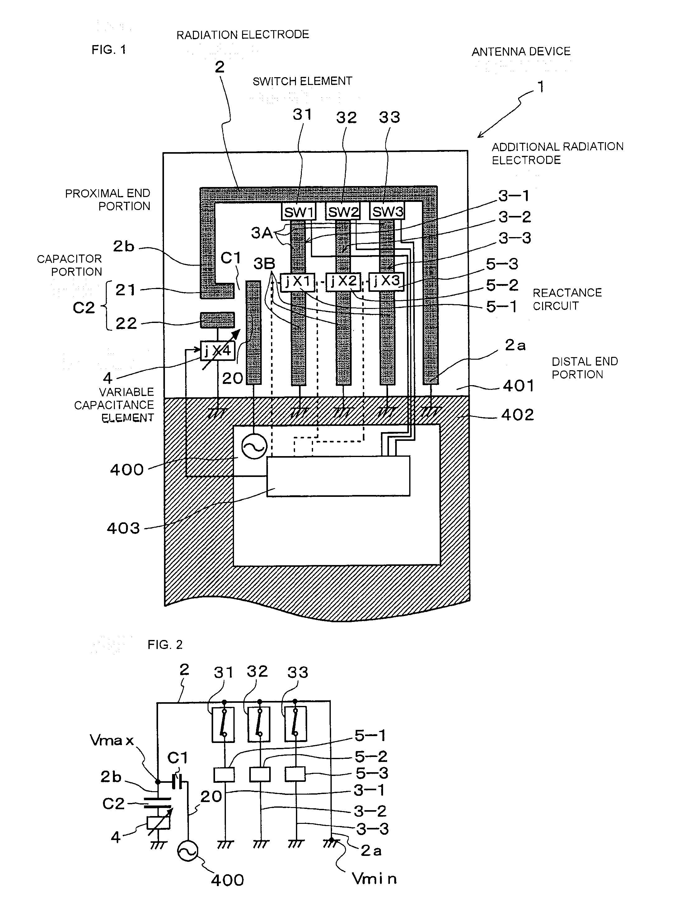
[0107]FIG. 1 is a plan view showing an antenna device according to a first embodiment.

[0108]An antenna device 1 of this embodiment is mounted in a wireless communication apparatus such as a mobile telephone or a PC card.

[0109]As shown in FIG. 1, the antenna device 1 is disposed in a non-ground region 401 on a circuit board of the wireless communication apparatus, and exchanges a high-frequency signal with a transmission / reception unit 400 serving as a feed unit mounted in a ground region 402.

[0110]The antenna device 1 includes a radiation electrode 2, and a plurality of additional radiation electrodes 3-1 to 3-3 branched from the radiation electrode 2.

[0111]The radiation electrode 2 is a conductive pattern that is bent into a right-angled U-shape. A distal end portion 2a of the radiation electrode 2 is grounded to the ground region 402.

[0112]High-frequency power is capacitively fed from the feed unit 400 to the radiation electrode 2. Specifically, a horizontal electrode portion 21 i...

second embodiment

[0137]Next, a second embodiment will be described.

[0138]FIG. 7 is a plan view showing an antenna device according to the second embodiment.

[0139]In the antenna device of this embodiment, the switch elements 31 to 33, the reactance circuits 5-1 to 5-3, and the variable capacitance element 4 of the first embodiment are implemented by specific elements.

[0140]As shown in FIG. 7, the switch elements 31 to 33 are implemented by Schottky diodes 31 to 33. Anodes of the Schottky diodes 31 (32 and 33) are connected to the radiation electrode 2 and cathodes thereof are connected to the electrode portions 3A of the additional radiation electrodes 3-1 (3-2 and 3-3).

[0141]The variable capacitance element 4 is implemented by a varicap 41. A cathode of the varicap 41 is connected to the electrode portion 22 and an anode thereof is grounded.

[0142]The reactance circuits 5-1 to 5-3 are implemented by inductors 51, and both ends of each of the inductors 51 are connected to the electrode portions 3A and...

third embodiment

[0151]Next, a third embodiment will be described.

[0152]FIG. 8 is a plan view showing an antenna device according to the third embodiment, FIG. 9 is a schematic view showing two resonance states, and FIG. 10 is a diagram showing a return loss curve obtained by two resonant frequencies.

[0153]The antenna device of this embodiment is different from the antenna devices of the first and second embodiments in that at least one reactance circuit of the reactance circuits 5-1 to 5-3 of the additional radiation electrodes 3-1 to 3-3 is formed of a capacitor.

[0154]Specifically, as shown in FIG. 8, the reactance circuit 5-1 is formed of a capacitor 52, and each of the reactance circuits 5-2 and 5-3 is formed of an inductor 51.

[0155]With this structure, when the switch element 31 of the additional radiation electrode 3-1 provided with the capacitor 52 is turned on, the inductors 51 of the additional radiation electrodes 3-2 and 3-3 that operate near the additional radiation electrode 3-1 and the...


PUM


Abstract

An antenna device capable of not only achieving multiple resonances and wideband characteristics but also achieving improvement of antenna efficiency and accurate matching at all resonant frequencies, and a wireless communication apparatus. In one example, an antenna device 1 includes a radiation electrode 2 to which power is capacitively fed through a capacitor portion C1, and additional radiation electrodes 3-1 to 3-3 branched from the radiation electrode 2. A distal end portion 2a of the radiation electrode 2 is grounded to a ground region 402, and is a portion at which a minimum voltage is obtained when power is fed. A capacitor portion C2 that is a portion at which a maximum voltage is obtained when power is fed is disposed in a proximal end portion 2b of the radiation electrode 2, and a variable capacitance element 4 which is grounded is connected in series with the capacitor portion C2. The additional radiation electrodes 3-1 to 3-3 are connected to the radiation electrode 2 through switch elements 31 to 33, and include reactance circuits 5-1 to 5-3 in a middle thereof. Distal end portions of the additional radiation electrodes 3-1 to 3-3 are grounded to the ground region 402.

Description

CROSS-REFERENCE TO RELATED APPLICATIONS[0001]The present application is a continuation of PCT / JP2007 / 062891, filed 27 Jun. 2007, which claims priority of Japanese Application No. 2006-206983, filed 28 Jul. 2006, both incorporated by reference herein. The PCT International Application was published in the Japanese language.BACKGROUND[0002]1. Technical Field[0003]An antenna device for use in a compact mobile telephone or the like and capable of multiple-resonance wideband transmission and reception, and to a wireless communication apparatus.[0004]2. Background Art[0005]In the related art, antenna devices of this type include the antenna devices shown in FIGS. 19 to 21.[0006]FIG. 19 is a plan view showing a multiple-resonance antenna device of the related art, FIG. 20 is a plan view of a wideband antenna device of the related art, and FIG. 21 is a plan view showing a multiple-resonance wideband antenna device of the related art.[0007]First, the antenna device 100 shown in FIG. 19 is an...

Claims


Application Information

Patent Timeline
Patent Type & Authority Applications(United States)
IPC IPC(8): H01Q9/00H01Q1/24
CPCH01Q1/243H01Q1/38H01Q5/00H01Q9/14H01Q5/49H01Q9/42H01Q5/328H01Q5/371H01Q9/38
Inventor ISHIZUKA, KENICHIKAWAHATA, KAZUNARITSUBAKI, NOBUHITO
Owner MURATA MFG CO LTD
Why Eureka
Try Eureka