Optically connectable circuit board with optical component(s) mounted thereon

a technology of optical components and circuit boards, applied in the direction of orthogonal pcbs mounting, electrical apparatus construction details, instruments, etc., can solve the problems of inability to meet the power requirements, dramatic cost increases, and signal loss at each tap point, so as to improve onboard communication

Inactive Publication Date: 2006-08-22
GLOBALFOUNDRIES INC
View PDF7 Cites 38 Cited by
  • Summary
  • Abstract
  • Description
  • Claims
  • Application Information

AI Technical Summary

Problems solved by technology

This is an unacceptable power requirement, particularly when tens of signals are required for a typical data path and well in excess of what is usually allowed for data communications optical paths.
Each of these three state of the art approaches produce incremental improvements only with solving difficult engineering problems accompanied by sometimes dramatic cost increases.
However, with the boards 302 connected to “tap points” along the backplane optical channels, some signal is lost at each tap point.
Clearly, the added work and expense has not provided for inclusion of more than a few more boards.
For thousand of signals (instead of tens of signals), the total power required is prohibitive.
Furthermore, such a 4 to 5 board system would be inflexible, unscalable beyond 5 boards.
Likewise removing 1 or 2 boards for a midrange system would not scale particularly easily either.
Signal integrity and radiation issues would arise in the infrastructure which is designed for the 4–5 board system.

Method used


Image

  • Optically connectable circuit board with optical component(s) mounted thereon
  • Optically connectable circuit board with optical component(s) mounted thereon
  • Optically connectable circuit board with optical component(s) mounted thereon

Examples


embodiment 900

[0049]FIG. 9 shows an example of an alternative embodiment grating structure 900 with like elements labeled identically. In this embodiment 900, the lasers 703, 705 are in the center of the chip 901 and a pair of identical photodiodes 902, 904 and gratings 906, 908 are located on either side of the lasers 703, 705. The two photodiodes 902, 904 are wired together (not shown) to act as a single photodiode. The advantage of this embodiment is that the photodiodes 902, 904 can sense light in the channel that was transmitted by this same chip, which may be used in testing. When a board is inserted into the backplane, a continuity check can be done using this embodiment.

[0050]FIG. 10 shows an example of a structure 1000 for coupling an optical signals from external light source / sink to the on-backplane transceivers 701. In this example, a second chip 1003 is flip mounted back to back with on-backplane transceivers 701. The second chip 1003 also contains a laser 1013 and a photodiode 1009 ...
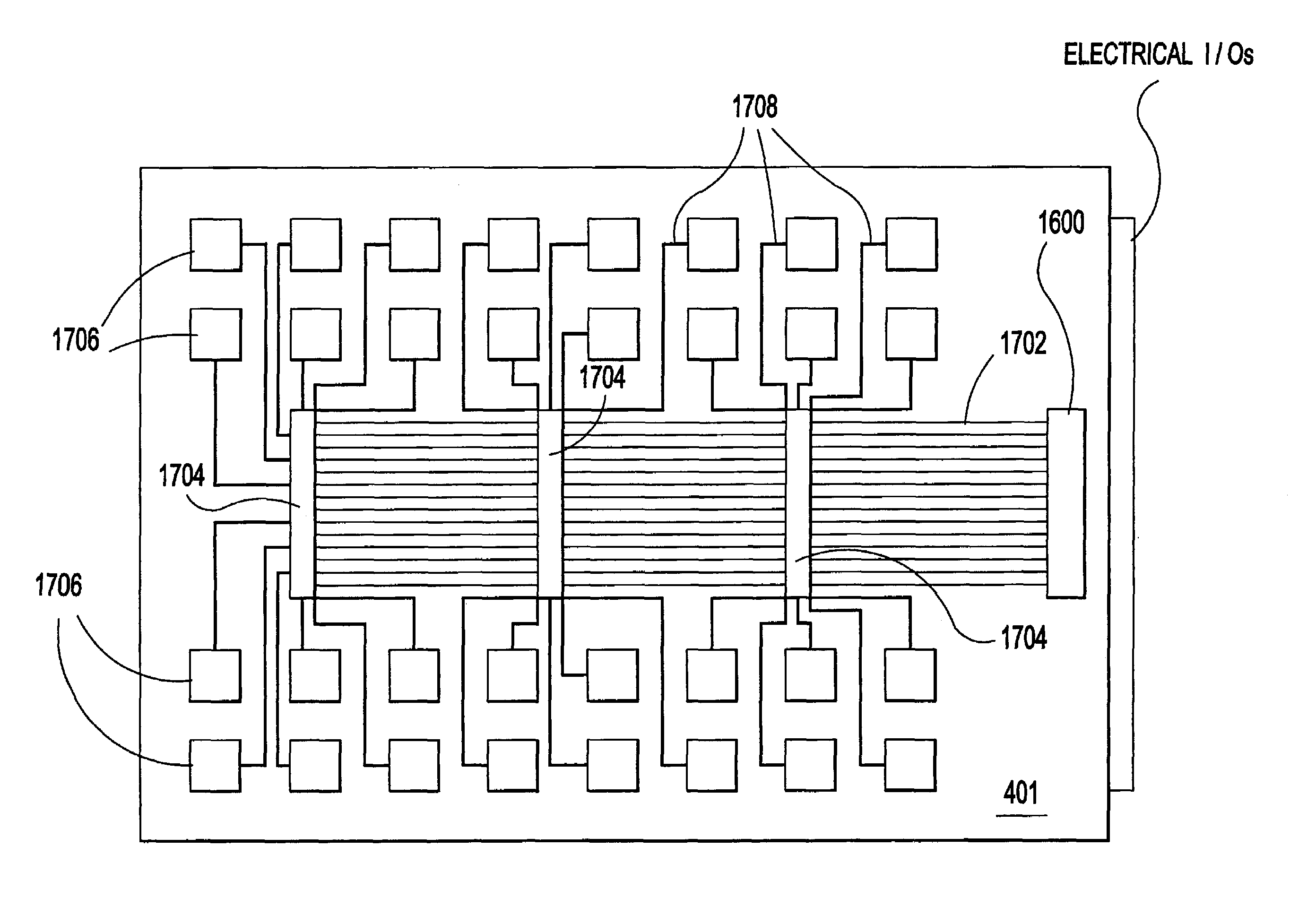
embodiment 401

[0055]FIG. 13 shows an example of board-to-backplane connector assembly 1300 mounted on a preferred embodiment 401 according to the present invention. A board-backplane optical jumper 1310 includes a pair of plugs 1201 and 1302 attached to either end of optical cables 1203, 1205 and connects the preferred circuit board 401 to a backplane (not shown in this example). Spring clamps on board optical sockets 1303 hold the board plug 1302 in place to provide an optical connection to an onboard transceiver structure 1304 as described hereinbelow and, substantially similar to a transceiver, e.g., 1000 in FIG. 10. A spring 1309 attaches across the optical jumper 1310 to provide tension for adequate optical coupling and to maintain plug 1201 inserted into a backplane optical socket.

[0056]FIG. 14 shows an example of a preferred board 401 attached to the backplane 403. The board 401 is inserted on an edge into a typical electrical edge connector 1409 on the backplane 403. An optical jumper 131...


PUM


Abstract

An optically connectable circuit board and optical components mounted thereon. At least one component includes optical transceivers and provides an optical connection to the board. Electronic components may be directly connected to the board electrically or optically. Also, some electronic components may be indirectly connected optically to the board through intermediate optical components.

Description

CROSS REFERENCE TO RELATED APPLICATIONS[0001]The present application is related to U.S. patent application Ser. No. 10 / 305,516 entitled “HIGH SPEED DATA CHANNEL INCLUDING A CMOS VCSEL DRIVER AND A HIGH PERFORMANCE PHOTODETECTOR AND CMOS PHOTORECEIVER” to Boszo et al., and U.S. patent application Ser. No. 10 / 31,585 entitled “BACKPLANE ASSEMBLY WITH BOARD TO BOARD OPTICAL INTERCONNECTIONS” to Boszo et al., both filed coincident herewith and both assigned to the assignee of the present invention.BACKGROUND OF THE INVENTION[0002]1. Field of the Invention[0003]The present invention generally relates to high-speed inter chip optical connections and more particularly to high speed optical inter board connections between logic and / or memory chips on different printed circuits, e.g., connected to a backplane.[0004]2. Description of the Related Art[0005]FIG. 1 shows an example of a state of the art electro-optical assembly 100 with a passive backplane 101 connecting two circuit boards 103 eac...

Claims


Application Information

Patent Timeline
Patent Type & Authority Patents(United States)
IPC IPC(8): H05K7/10H05K7/12H05K1/14G02B6/12G02B6/122G02B6/124G02B6/38G02B6/42G02B6/43H05K1/02
CPCG02B6/12004G02B6/124G02B6/3885G02B6/43H05K1/0274G02B6/4292G02B6/4246H05K2201/044H05K1/14H01L2224/16225H01L2224/73204H01L2924/15311
Inventor BOZSO, FERENC M.EMMA, PHILIP G.
Owner GLOBALFOUNDRIES INC
Why Eureka
Try Eureka