Resistor structure and method for manufacturing the same

a resistor and structure technology, applied in the field of resistor structure, can solve the problems of increasing the complexity of circuit design applying load resistors, increasing the difficulty in calculating an accurate value of resistance, and decreasing the yield of products, so as to reduce the end resistance of resistor structure, stable high resistance, and improve the yield of products

Active Publication Date: 2006-09-12
UNITED MICROELECTRONICS CORP
View PDF3 Cites 6 Cited by
  • Summary
  • Abstract
  • Description
  • Claims
  • Application Information

AI Technical Summary

Benefits of technology

[0010]It is an advantage of the present invention that the doping concentration in the vicinity of the junction between the high resistance region and the low resistance region is increased to reduce the end-resistance of the resistor structure. Therefore, problems such as unstable resistance resulted from the doping concentration variation as occurred in the vicinity of the junction between the high resistance region and the low resistance region in the prior art resistor structure can be effectively prevented. A stable high resistance is thus provided to improve yields of the products according to the present invention.
[0011]These and other objects of the claimed invention will be apparent to those of ordinary skill in the art after reading the following detailed description of the preferred embodiment that is illustrated in the various figures and drawings.

Problems solved by technology

With the development of the various electronic products, circuit designs applying load resistors become more and more complicated.
In this case, it becomes more difficult to calculate an accurate value of the resistance and provide a stable value of high resistance, thus decreasing yields of the products.

Method used


Image

  • Resistor structure and method for manufacturing the same
  • Resistor structure and method for manufacturing the same
  • Resistor structure and method for manufacturing the same

Examples


Embodiment Construction

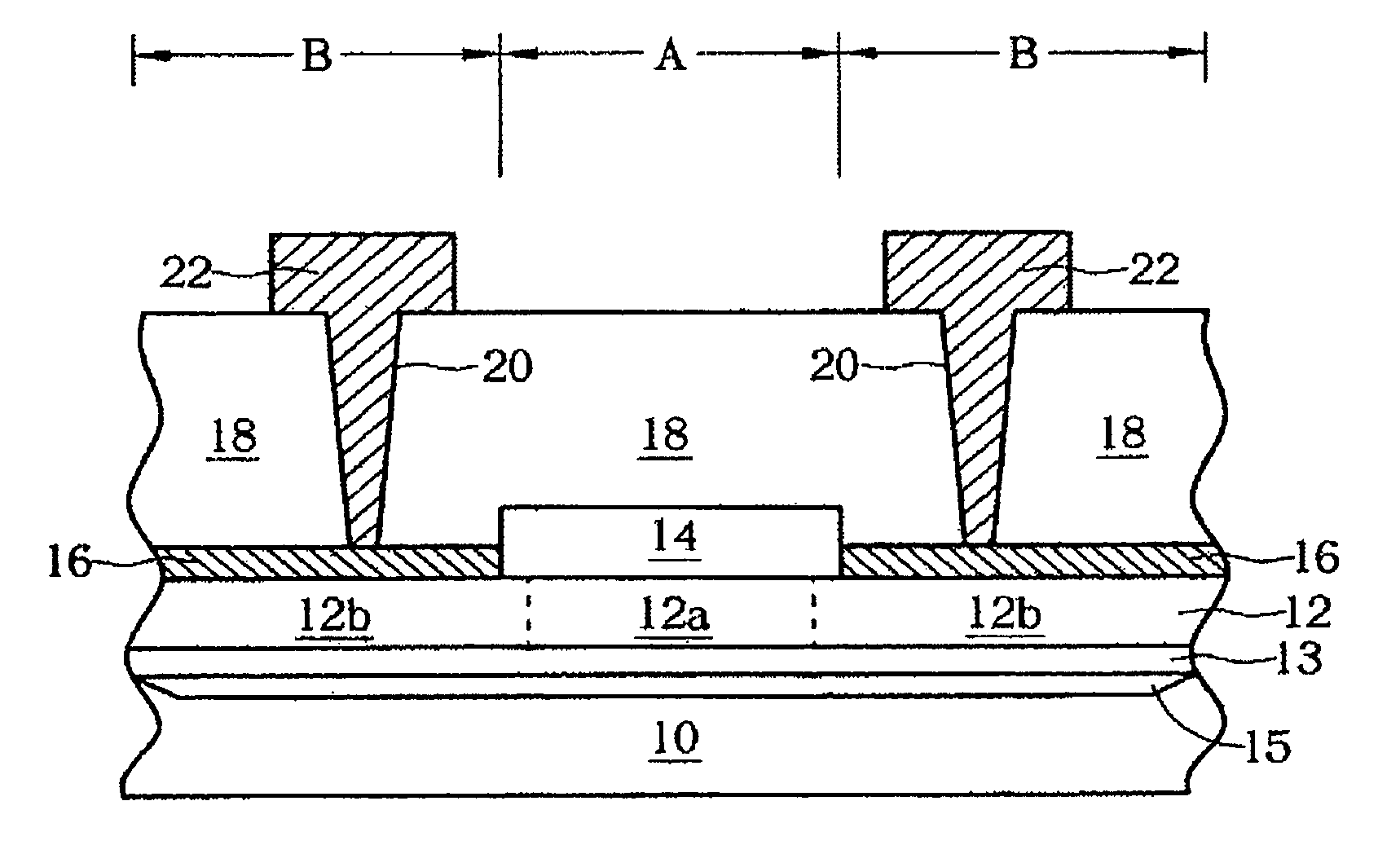
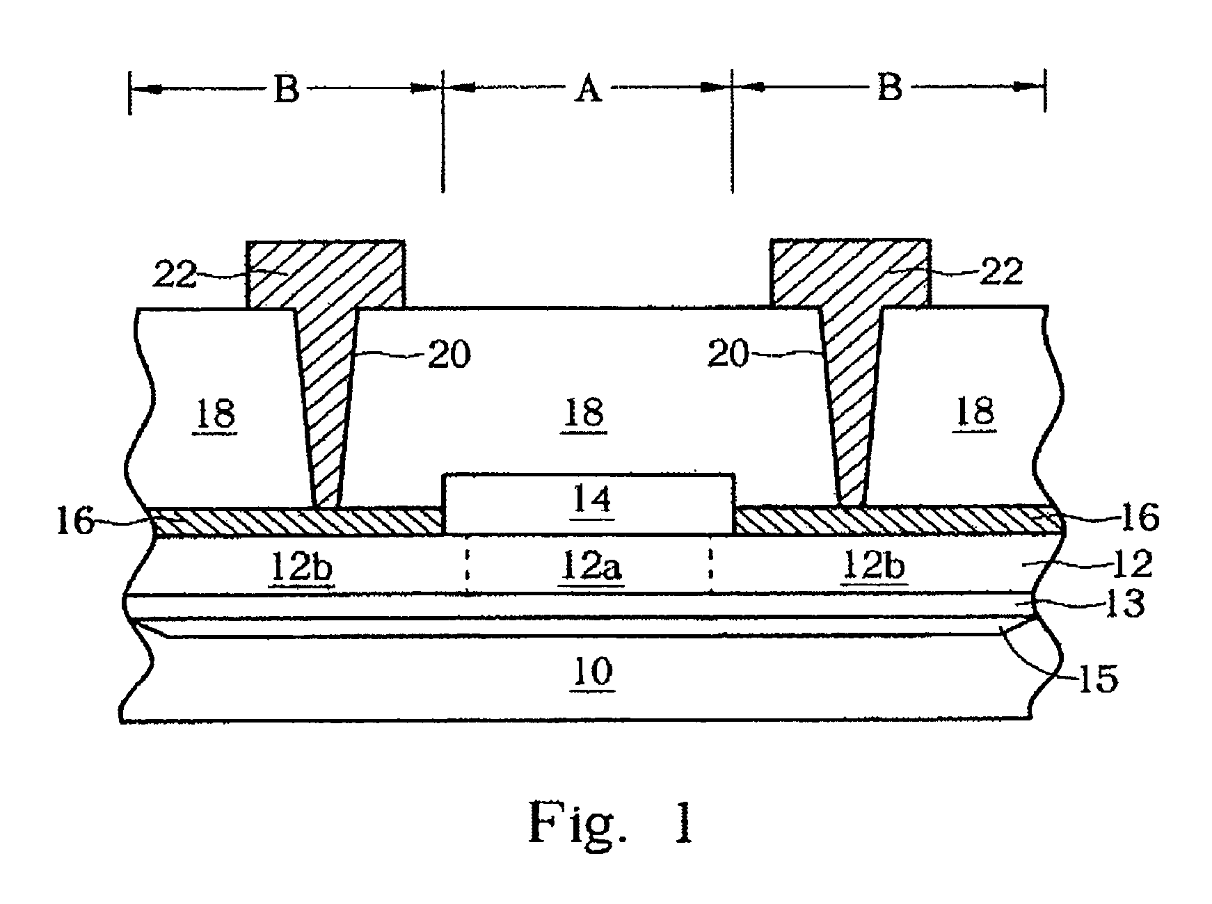
[0014]Referring to FIG. 1, FIG. 1 is a cross-sectional diagram of a resistor structure according to the present invention. As shown in FIG. 1, the resistor structure includes a substrate 10, and a semiconductor layer 12 positioned on the substrate 10. The semiconductor layer 12 has a high resistance region A and at least a low resistance region B positioned at either side of the high resistance region A. In order to prevent problems of unstable resistance from occurring in the vicinity of the junction between the high resistance region A and the low resistance region B, the semiconductor layer 12 has a lightly doped region 12a formed within the high resistance region A, and at least a heavily doped region 12b overlapping the low resistance region B, the junction between the high resistance region A and the low resistance region B, and the portions of the high resistance region A adjacent to the junction between the high resistance region A and the low resistance region B. The semico...


PUM


Abstract

A resistor structure includes a substrate, a semiconductor layer positioned on the substrate, a salicide block positioned on portions of the surface of the semiconductor layer, and at least a salicide layer positioned on the portions of the surface of the semiconductor layer adjacent to the salicide block. The semiconductor layer has a predetermined region overlapping the salicide layer, the junction between the salicide layer and the salicide block, and the portions of the salicide block adjacent to the junction between the salicide layer and the salicide block. The semiconductor layer has a higher doping concentration within the predetermined region than in the other regions.

Description

BACKGROUND OF INVENTION[0001]1. Field of the Invention[0002]The present invention relates to a resistor structure and a method for manufacturing the same, and more particularly, to a resistor structure having low end-resistance and a method for manufacturing the same.[0003]2. Description of the Prior Art[0004]In a semiconductor process, semiconductor materials, such as polysilicon, are often positioned to function as resistors capable of providing high resistance. These resistors can be used in place of load transistors. When load transistors of a static random access memory (SRAM) is replaced by semiconductor resistors, the number of transistors in the SRAM can be reduced and thus saves cost and enhance the integration of the SRAM.[0005]Conventionally used semiconductor resistors can be divided into polysilicon resistors and diffusion resistors. A polysilicon resistor is formed, for example, by forming a polysilicon film into which dopants are doped into through an insulating film ...

Claims


Application Information

Patent Timeline
Patent Type & Authority Patents(United States)
IPC IPC(8): H01L29/00
CPCH01L29/8605
Inventor CHEN, CHENG-HSIUNGLEE, YUE-SHIUN
Owner UNITED MICROELECTRONICS CORP
Why Eureka
Try Eureka