
Polysilicon resistor semiconductor device

Inactive Publication Date: 2006-10-10
FUJI ELECTRIC CO LTD
View PDF18 Cites 6 Cited by
  • Summary
  • Abstract
  • Description
  • Claims
  • Application Information

AI Technical Summary

Benefits of technology

[0012]According to the present invention, the resistance value Rcon of the polysilicon contact is reduced to 2% or less of the sum of the resistance value Rcon of the polysilicon contact and the re

Problems solved by technology

The adverse effects of temperature have not been sufficiently examined, so that specific constraints on temperature and the like are unknown.
All of these proposals attempt to realize, during the manufacturing stage, a resistance value as close to a design value as possible, and are not intended to suppress variations over time in resistance value in high-temperature environments.
Accordingly, if such a semiconductor device composed of a conventional polysilicon resistor is used in an amplifying circuit used in high-temperature environments, amplifying rate varies over time in this high-temperature environment, making it difficult to maintain reliability over an extended period.

Method used


Image

  • Polysilicon resistor semiconductor device
  • Polysilicon resistor semiconductor device
  • Polysilicon resistor semiconductor device

Examples


Embodiment Construction

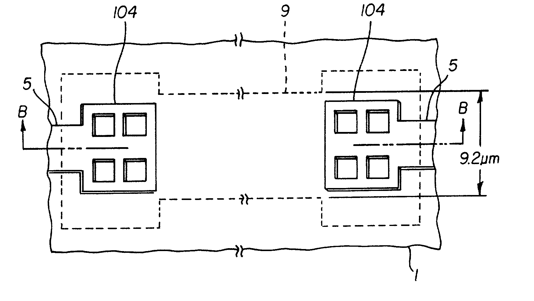
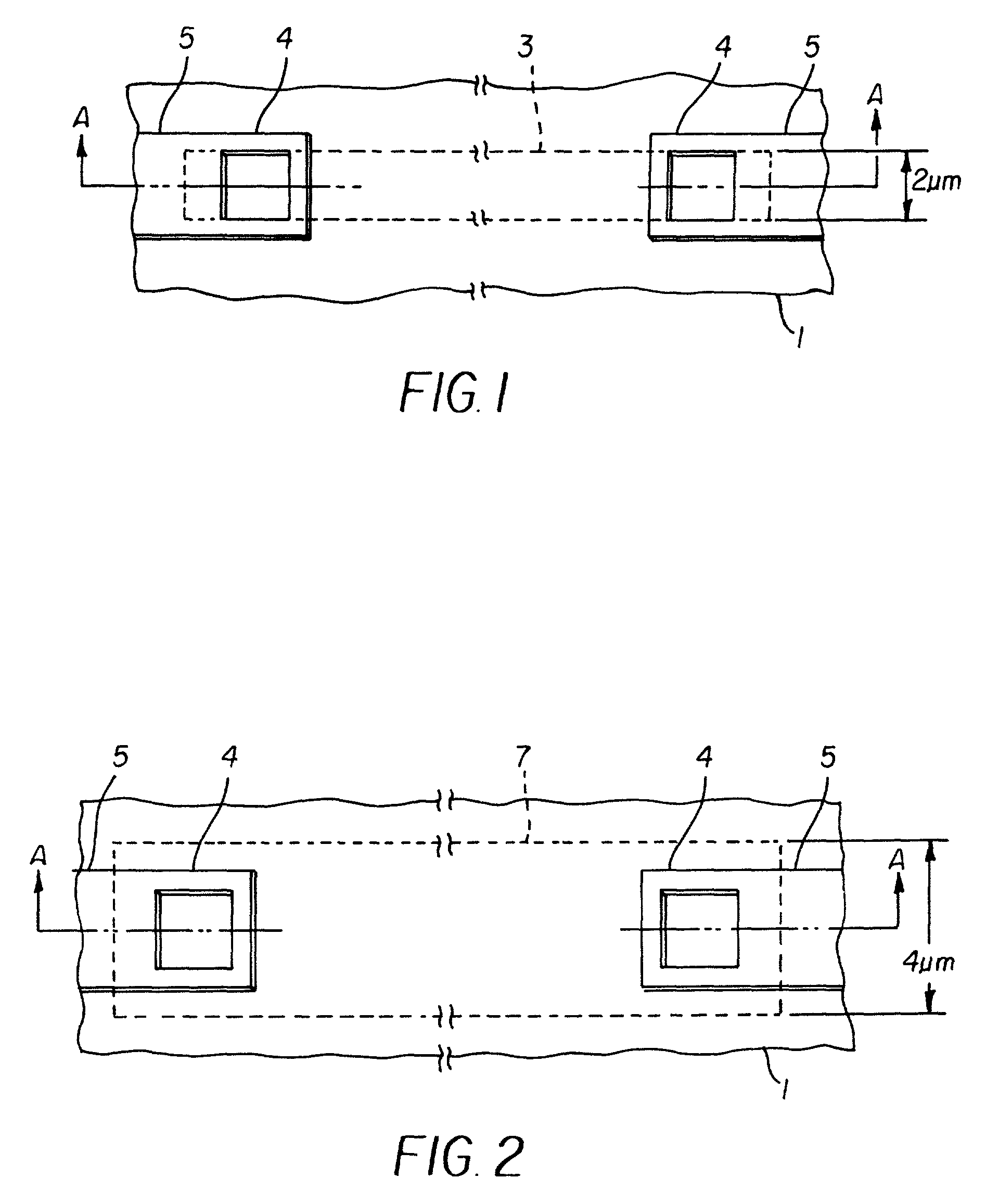
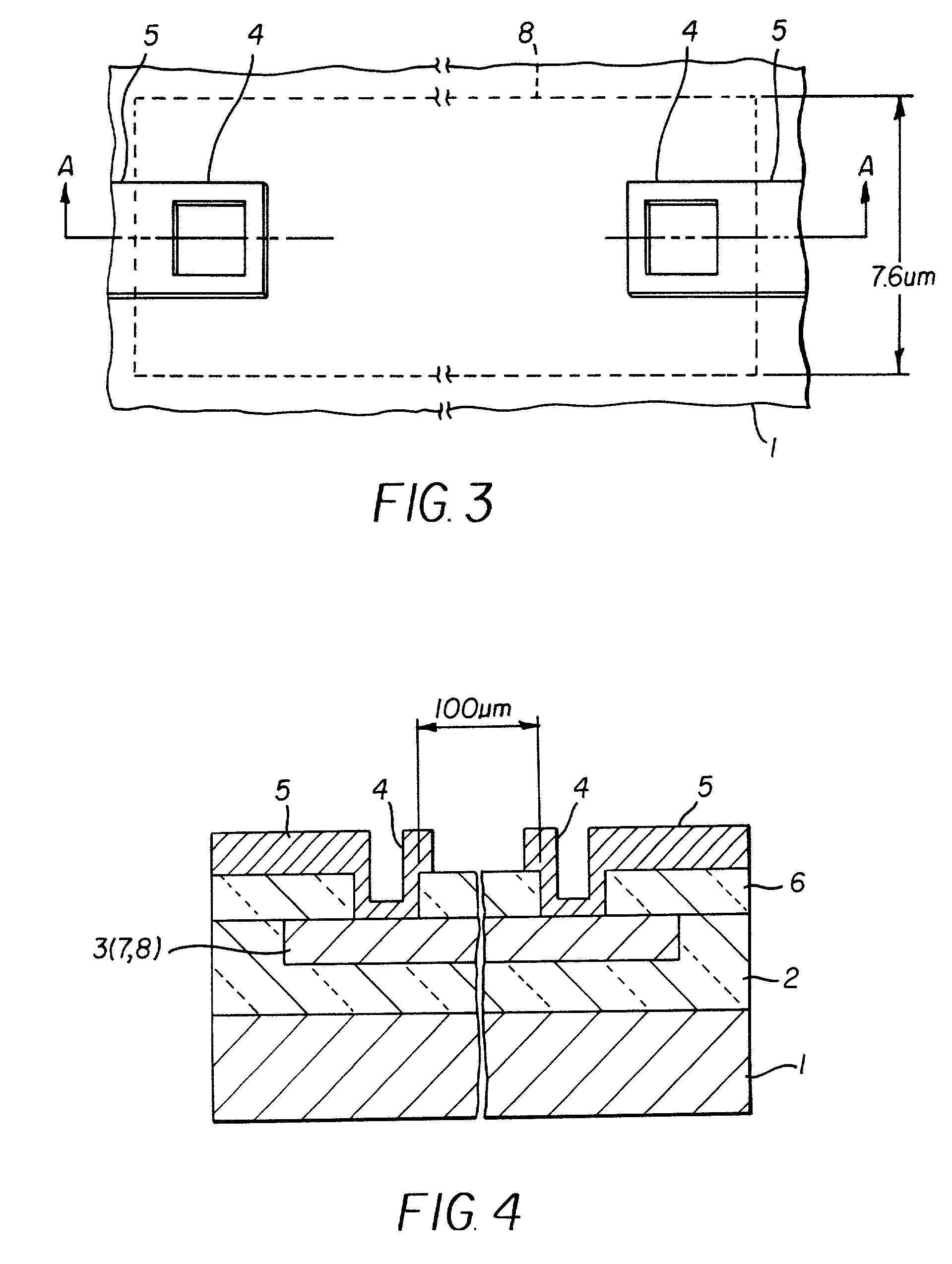
[0023]In accordance with the present invention, four polysilicon resistor semiconductor devices comprising a first, a second, a third, and a fourth device, described below, were prepared. FIGS. 1 to 3 consist of plan views schematically showing the configurations of the semiconductor devices comprising the first, second, and third polysilicon resistors. These three semiconductor devices have the same configurations, except for the width and the resistance value of the polysilicon resistor. Accordingly, these semiconductor devices have the same vertically sectional structure along line A—A in FIGS. 1 to 3, as shown in FIG. 4. FIGS. 5 and 6 consist of plan views of the fourth polysilicon resistor semiconductor device, schematically showing the configuration of the device and a vertical sectional view taken along line B—B, respectively. In FIGS. 1 to 6, the relative sizes and lengths of the components are not drawn to scale.

[0024]As shown in FIGS. 1 and 4, the polysilicon resistor semi...


PUM


Abstract

A semiconductor device includes a polysilicon resistor that can suppress variations in resistance value in environments with an ambient temperature higher than room temperature. The resistance value Rcon of a polysilicon contact is reduced to 2% or less of the sum of the resistance value Rcon of the polysilicon contact and the resistance value Rpoly of a polysilicon resistor. Hence, a semiconductor device that is not significantly affected by a variation in the resistance of the polysilicon contact is realized. This device suppresses variations in resistance value in environments with an ambient temperature higher than room temperature.

Description

FIELD OF THE INVENTION[0001]The present invention relates to a semiconductor device, and in particular, to a semiconductor device comprising a polysilicon resistor used as a resistance element in various semiconductor integrated circuits for automobiles, measurements, or calibrations that are used in high-temperature environments.BACKGROUND OF THE INVENTION[0002]In a semiconductor integrated circuits, factors affecting the occurrence of electromigration, which may deform a conductor or cause the circuit to malfunction, are known to include element density, temperature, and crystal structure as explained in Takashi TOMIZAWA and Yasuo MATSUYAMA “Principle Of COMOSVLS1 Design—From the Viewpoint Of Systems,” Maruzen Co., Ltd., pp. 122, incorporated herein by reference. The adverse effects of temperature have not been sufficiently examined, so that specific constraints on temperature and the like are unknown.[0003]For semiconductor integrated circuits used for automobiles or plant measur...

Claims


Application Information

Patent Timeline
IPC IPC(8): H01C1/012H01C7/06H01L27/02H01L21/02H01L23/522H01L27/08
CPCH01L23/522H01L27/0802H01L28/20H01L2924/0002H01L2924/00H01L27/02
Inventor UEYANAGI, KATSUMICHINISHIKAWA, MUTSUOUEMATSU, KATSUYUKI
Owner FUJI ELECTRIC CO LTD
Learn More