
Capacitive type touch panel

a capacitive touch panel and capacitive type technology, applied in the field of capacitive touch panel, can solve the problems of difficult to calculate accurate coordinates, the electrode structure of the conventional capacitive touch panel, and the inability of input devices including only a keyboard and a mouse to deal with the extended use of products, etc., to achieve the effect of enhancing response speed and touch sensitivity

Inactive Publication Date: 2017-03-02
ABOV SEMICON
View PDF1 Cites 0 Cited by
  • Summary
  • Abstract
  • Description
  • Claims
  • Application Information

AI Technical Summary

Benefits of technology

This patent describes a capacitive touch panel that improves response speed and touch sensitivity by reducing the resistance value of the top transparent electrodes. The panel includes a linear electrode and pattern electrodes that create a space-saving design. Additionally, the panel provides accurate coordinate values even with a small number of electrodes and reduces manufacturing costs and improves the manufacturing yield of products.

Problems solved by technology

Input devices including only a keyboard and a mouse cannot deal with the extended uses of products, such as PCs, as input devices used for interfaces.
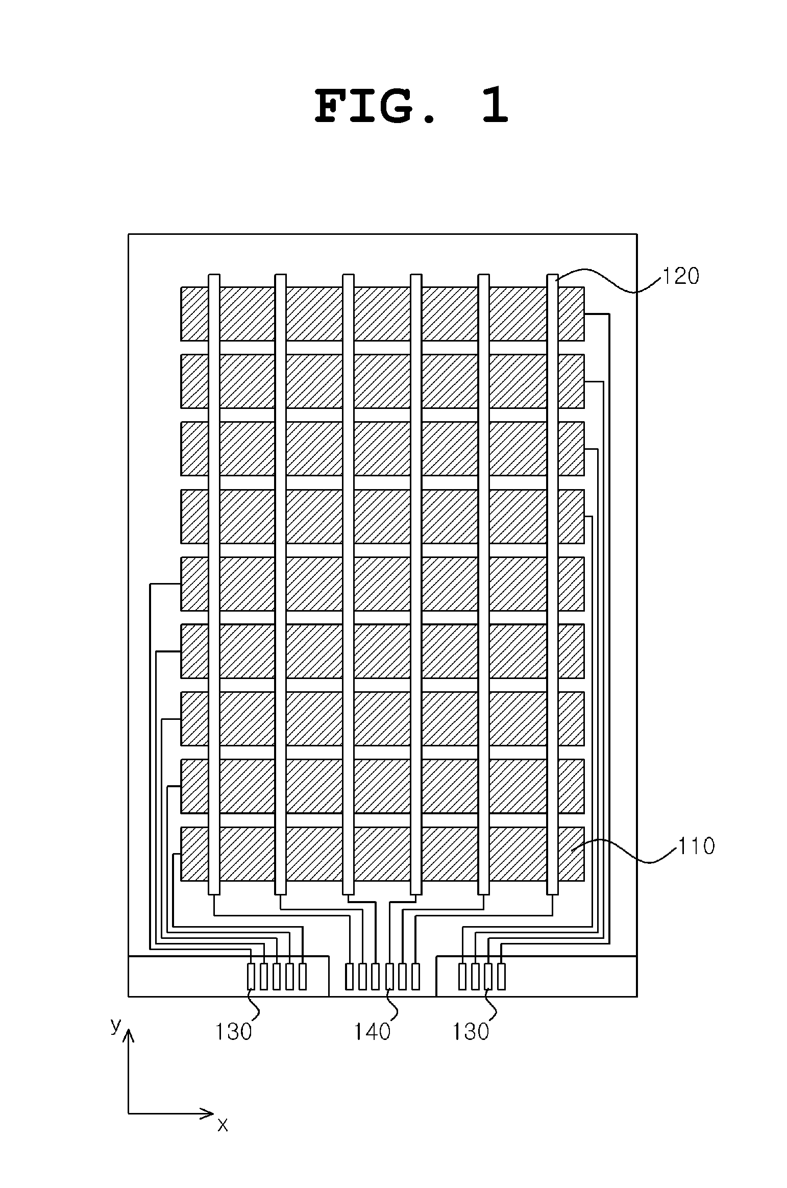
However, when the number of electrodes or electrode terminals available in the structure of the conventional capacitive touch panel is insufficient, the electrodes are arranged at wider intervals, for example, intervals of 10 mm.
In this case, a problem arises in that it becomes difficult to identify contact with the human body, with the result that it becomes difficult to calculate accurate coordinates.
That is, the electrode structure of the conventional capacitive touch panel has a problem in that it cannot guarantee coordinate linearity.

Method used


Image

  • Capacitive type touch panel
  • Capacitive type touch panel
  • Capacitive type touch panel

Examples


Embodiment Construction

[0043]Embodiments of the present invention will be described in detail with reference to the accompanying drawings. In the following description of the present invention, detailed descriptions of related well-known components or functions that may unnecessarily make the gist of the present invention obscure will be omitted.

[0044]The prevent invention is not limited to the embodiments. Throughout the accompanying drawings, the same reference symbols are assigned to the same components.

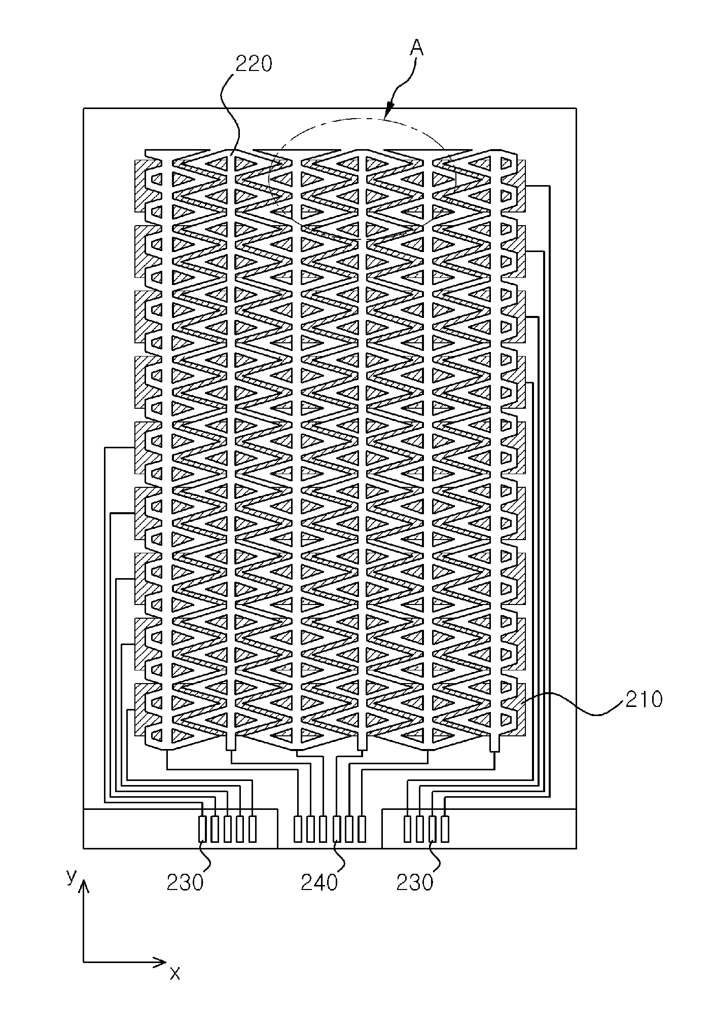
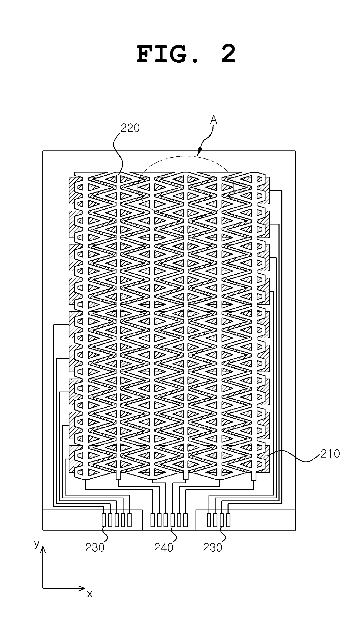
[0045]A capacitive touch panel according to an embodiment of the present invention is described in detail below with reference to FIGS. 2 to 12.

[0046]The gist of the present invention resides in providing coordinate linearity even when the number of electrodes is small and thus providing the accurate coordinate values of a touched location, and also resides in reducing the total resistance value of electrodes, increasing a change in mutual capacitance attributable to a touch and thus improving response ...


PUM


Abstract

A capacitive touch panel is disclosed herein. The capacitive touch panel includes a plurality of bottom transparent electrodes formed in a first direction and a plurality of top transparent electrodes formed in a second direction perpendicular to the first direction. Each of the top transparent electrodes includes a linear electrode, a plurality of first pattern electrodes, and a plurality of second pattern electrodes. The linear electrode is linearly formed in the second direction. The plurality of first pattern electrodes is formed on the first side of the linear electrode in a predetermined first pattern, and is formed at predetermined intervals in an alternately protruding and recessed form in the second direction. The plurality of second pattern electrodes is formed on the second side of the linear electrode in a predetermined second pattern, and is formed at predetermined intervals in an alternately protruding and recessed form in the second direction.

Description

CROSS-REFERENCE TO RELATED APPLICATION[0001]This application is a continuation of PCT / KR2014 / 002782 filed on Apr. 1, 2014, which claims priority to Korean Application No. 10-2013-0036324 filed on Apr. 3, 2013, which application is incorporated herein by reference.TECHNICAL FIELD[0002]The present invention relates to a capacitive touch panel and, more particularly, to a capacitive touch panel that can reduce the total resistance value of top transparent electrodes, that can reduce the number of electrode terminals used for the top transparent electrodes, and that can provide the accurate coordinate values of a touched location through the guarantee of coordinate linearity.BACKGROUND ART[0003]Personal computers (PCs), portable transmission devices, and other personal dedicated information processing devices perform text and graphics processing and the like via various input devices, such as a keyboard, a mouse, and a digitizer.[0004]Input devices including only a keyboard and a mouse ...

Claims


Application Information

Patent Timeline
IPC IPC(8): G06F3/041G06F3/044
CPCG06F3/0418G06F2203/04104G06F3/044G06F3/0445G06F3/0446G06F3/0448
Inventor JEE, SEOK HYUN
Owner ABOV SEMICON
Learn More