Manufacturing method of pixel structure
a manufacturing method and pixel technology, applied in the direction of electrical equipment, semiconductor devices, instruments, etc., can solve the problems of obvious rc delay effect and display quality degradation, and achieve the effect of reducing the resistance value increasing the length of reducing the distance between scan lines and data lines
- Summary
- Abstract
- Description
- Claims
- Application Information
AI Technical Summary
Benefits of technology
Problems solved by technology
Method used
Image
Examples
first embodiment
The First Embodiment
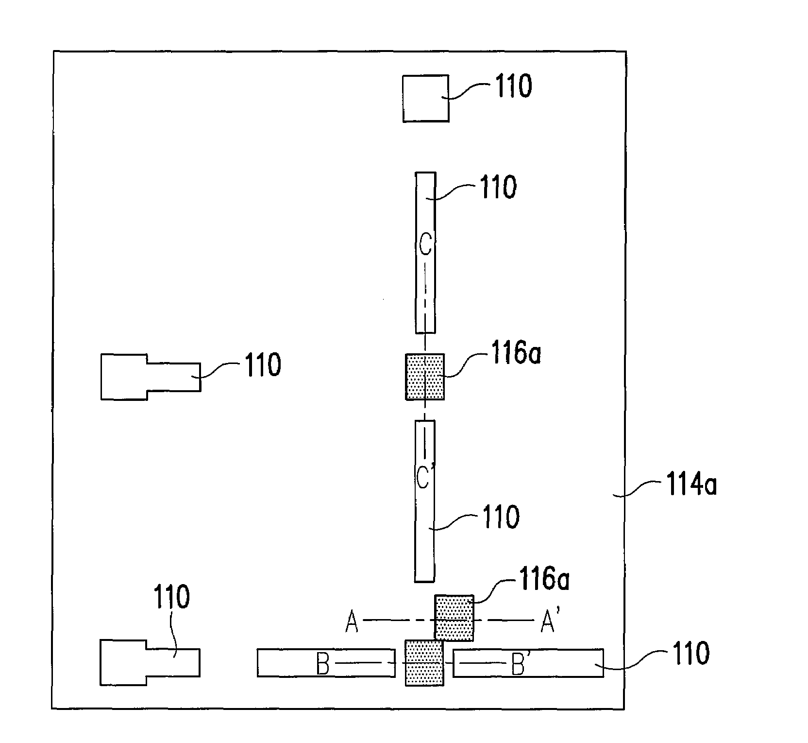
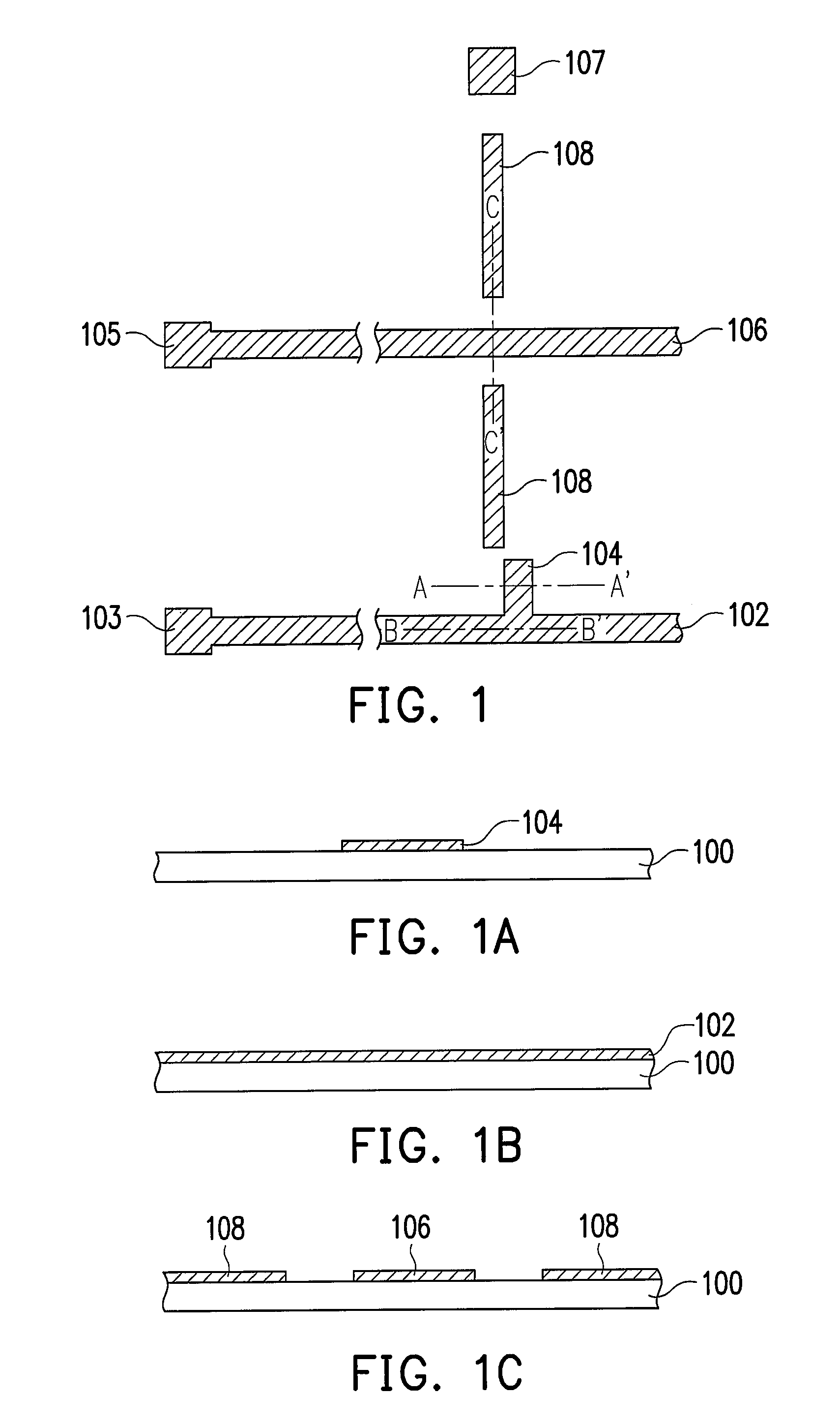
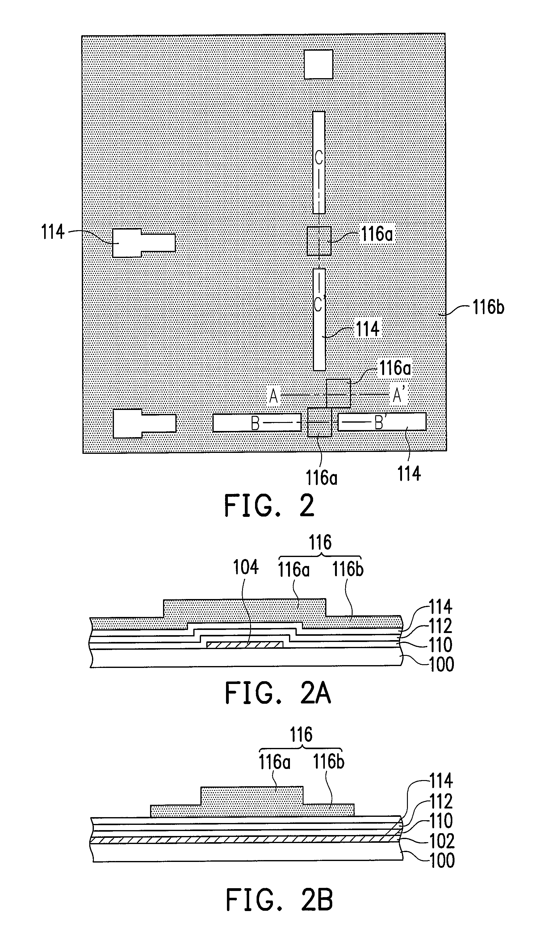
[0024]FIGS. 1-7 are top views of the method of manufacturing the pixel structure according to a preferred embodiment of the present invention, wherein FIGS. 1A, 2A, 3A, 4A, 5A, 6A, and 7A are cross-sectional views along Line A-A′ in the top views, respectively; FIGS. 1B, 2B, 3B, 4B, 5B, 6B, and 7B are cross-sectional views along Line B-B′ in the top views, respectively; and FIGS. 1C, 2C, 3C, 4C, 5C, 6C, and 7C are cross-sectional views along Line C-C′ in the top views, respectively. First, referring to FIGS. 1, 1A, 1B, and 1C, a scan line 102, a gate 104 connected to the scan line 102, and at least one first auxiliary pattern 108 are formed on a substrate 100. In a preferred embodiment, the aforementioned step further comprises forming a bottom electrode line 106 on the substrate 100. In another preferred embodiment, the aforementioned step further comprises forming a scan line terminal 103 connected to the scan line 102 on the substrate 100. Additionally, a bott...
second embodiment
The Second Embodiment
[0033]FIGS. 9-14 are top views of the method of manufacturing the pixel structure according to another preferred embodiment of the present invention, wherein FIGS. 9A, 10A, 11A, 12A, 13A, and 14A are cross-sectional views along Line A-A′ in the top views; FIGS. 9B, 10B, 11B, 12B, 13B, and 14B are cross-sectional views along Line B-B′; and FIGS. 9C, 10C, 11C, 12C, 13C, and 14C are cross-sectional views along Line C-C′. First, referring to FIGS. 9, 9A, 9B, and 9C, a scan line 102, a gate 104 connected to the scan line 102, and at least one first auxiliary pattern 108 are formed on a substrate 100. In a preferred embodiment, the aforementioned step further comprises forming a bottom electrode line 106 on the substrate 100. In another preferred embodiment, the aforementioned step further comprises forming a scan line terminal 103 connected to the scan line 102 on the substrate 100. Additionally, a bottom electrode terminal 105 connected to the bottom electrode line ...
PUM
 Abstract
Description
Claims
Application Information
 - R&D
- Intellectual Property
- Life Sciences
- Materials
- Tech Scout
- Unparalleled Data Quality
- Higher Quality Content
- 60% Fewer Hallucinations
Browse by: Latest US Patents, China's latest patents, Technical Efficacy Thesaurus, Application Domain, Technology Topic, Popular Technical Reports.
© 2025 PatSnap. All rights reserved.Legal|Privacy policy|Modern Slavery Act Transparency Statement|Sitemap|About US| Contact US: help@patsnap.com


