Method of setting process parameter and method of setting process parameter and/or design rule

a technology of process parameter and design rule, which is applied in the direction of diffusion transfer process, semiconductor/solid-state device testing/measurement, instruments, etc., can solve the problems of not meeting the specifications of the pattern, the pattern formed cannot be said to provide the desired device pattern, and the pattern is difficult to form

Inactive Publication Date: 2006-10-10
KIOXIA CORP
View PDF20 Cites 225 Cited by
  • Summary
  • Abstract
  • Description
  • Claims
  • Application Information

AI Technical Summary

Problems solved by technology

As patterns grow finer and more complex, however, it becomes difficult to form, on semiconductor wafers, patterns that accord with the design patterns.
In other words, the patterns formed can hardly satisfy the specifications.
In view of this, the method cannot be said to provide desired device patterns.
Hence, the conventional techniques described above can hardly serve to manufacture devices of such micro-patterns as is desired.
Consequently, it is difficult for the conventional methods to set appropriate process parameters and to form desirable patterns on semiconductor wafers.
A design layout prepared by using the design rule obtained by the method described above cannot always provide chips of desired sizes.
It is practically impossible, however, to allocate a particular design rule to each pattern.
The more design rules, the longer the time required to prepare a design layout, and the more complex the verification achieved by using a design rule checker (D.R.C.).
Unless appropriate design rules are allocated to all patterns to be formed, there may be formed dangerous patterns that fail to satisfy prescribed process latitude.
If the design rule is mitigated, the chip area will inevitably increase.
Hitherto, however, such a relation has not been fully applied to the preparation of masks.
Inevitably it has been difficult to set such optimal design rules or process parameters as would reduce the chip size as much as possible.
It is therefore difficult to set appropriate process parameters in the conventional methods.
Furthermore, it has been hard to set such design rules or such process parameters as would reduce the chip size to a minimum.
To this date it has been difficult to form desired patterns on semiconductor wafers.

Method used


Image

  • Method of setting process parameter and method of setting process parameter and/or design rule
  • Method of setting process parameter and method of setting process parameter and/or design rule
  • Method of setting process parameter and method of setting process parameter and/or design rule

Examples


first embodiment

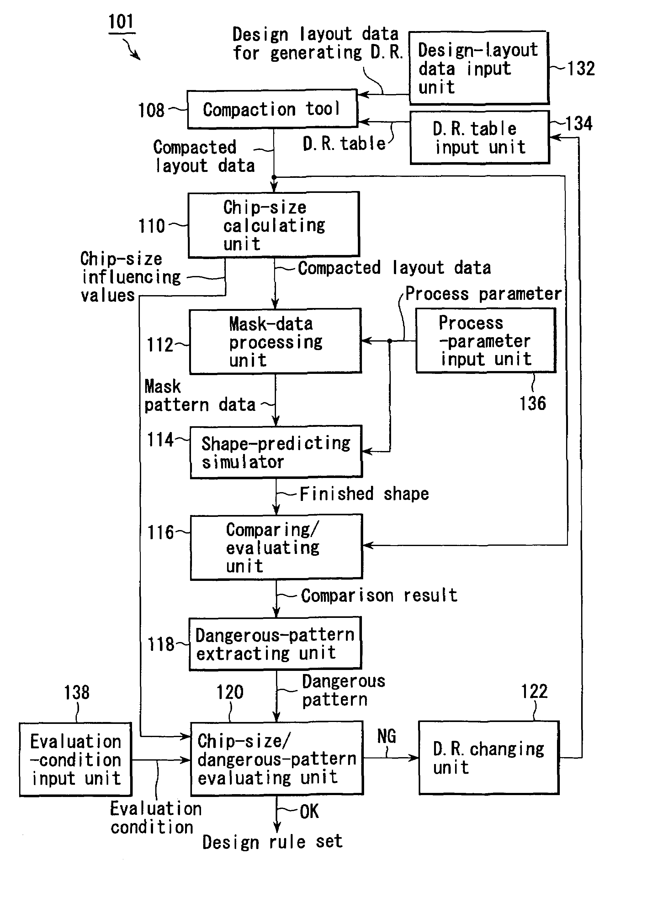
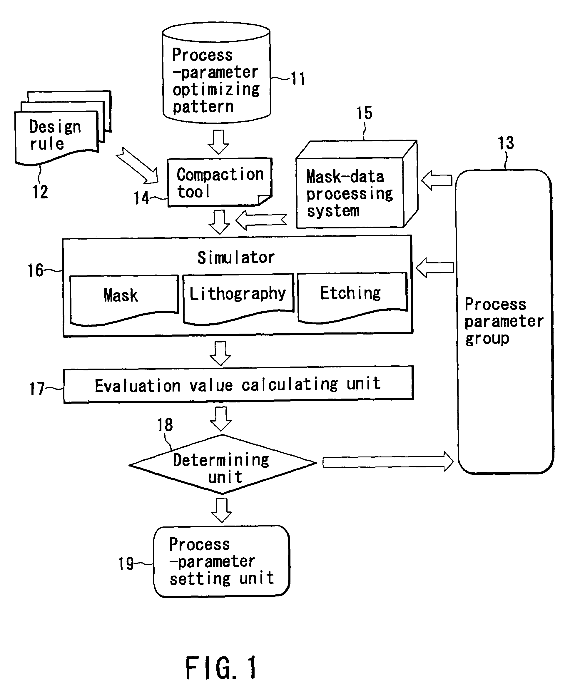
[0031]FIG. 1 is a function-block diagram of a process-parameter setting system according to the first embodiment of the present invention.

[0032]Process-pattern optimizing patterns 11, design rules 12 and parameter groups 13 are prepared for the process-parameter setting system. The parameter group 13 includes a plurality of process parameters.

[0033]The process-pattern optimizing patterns 11 include design layout patterns for use in various masks or reticles and are similar to patterns of actual devices. The design rules 12 are ones for use in manufacturing, for example, the next-generation devices.

[0034]Among the process parameters of the group 13 are parameters that influence the finished shapes of the patterns to be formed on a semiconductor substrate (semiconductor wafer). More precisely, some of the process parameters relate to the mask-forming process, some of the process parameters relate to the lithography process, and some of the process parameters relate to the etching proc...

second embodiment

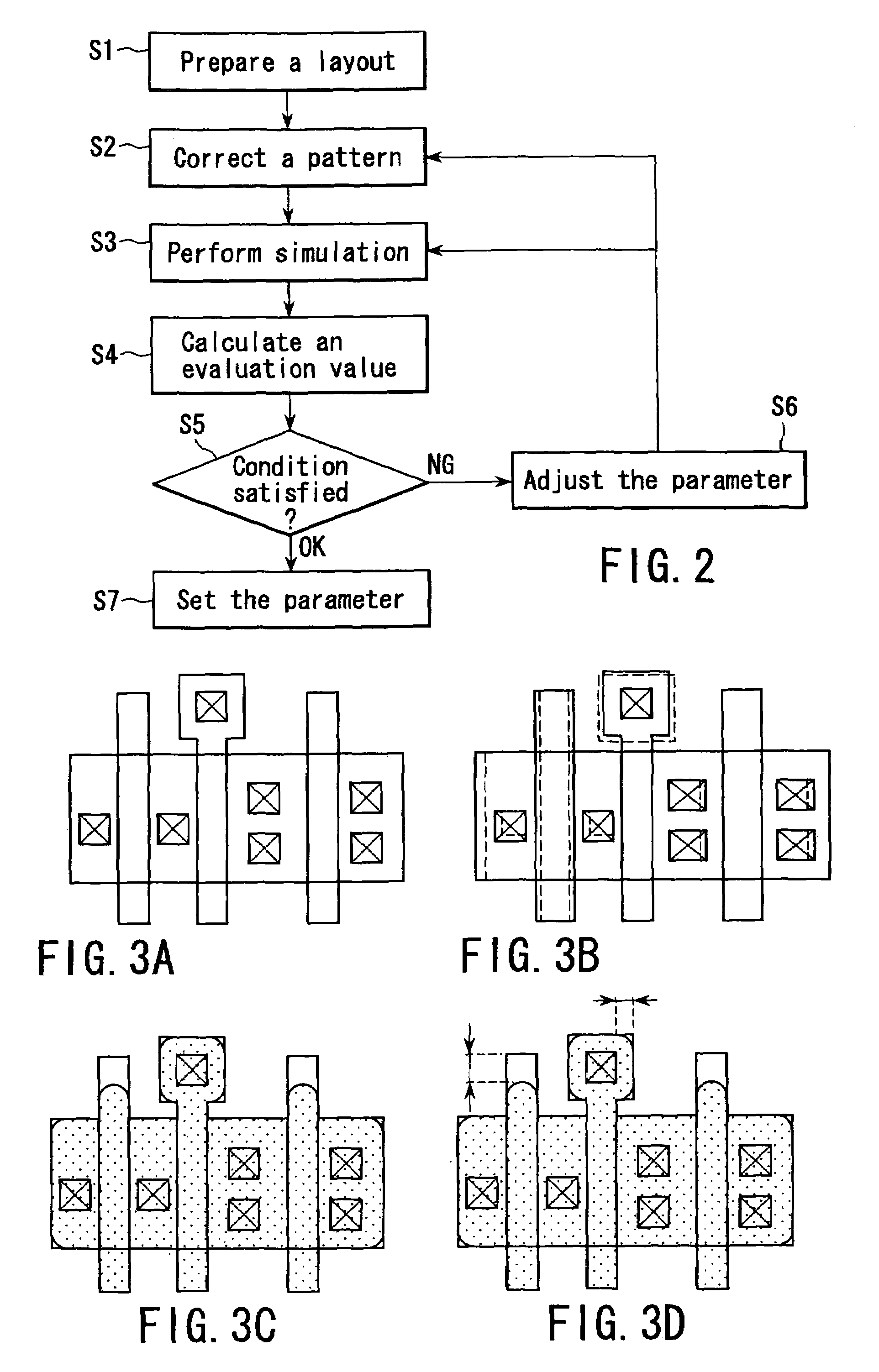
[0069]The basic concept of the second embodiment of the present invention will be explained first.

[0070]FIG. 7A is a schematic representation of the relation between the severity of design rules (D.R.), on the one hand, and the chip size and the number of dangerous patterns, on the other hand. The severity of D.R. is plotted on the abscissa, decreasing toward the right and increasing toward the left. The chip size and the number of dangerous patters are plotted on the upper half and lower half of the ordinate, respectively. As seen from Area AR1, if the D.R. severity is low, the number of dangerous patterns can be small, though the chip size is large. As seen from Area AR2, if the D.R. severity is high, the chip size can be small, though the number of dangerous patterns is large.

[0071]The chip size and the number of dangerous patterns are preset in accordance with the specifications of the device. Assume that the chip size is preset to A or less and the number of dangerous patterns ...


PUM


Abstract

Disclosed is a method of setting a process parameter for use in manufacturing a semiconductor integrated circuit, comprising correcting a first pattern by using process parameter information to obtain a second pattern, the first pattern being one which corresponds to a design layout of the semiconductor integrated circuit, predicting a third pattern by using the process parameter information, the third pattern being one which corresponds to the second pattern and which is to be formed on a semiconductor wafer in an etching process, obtaining an evaluation value by comparing the third pattern with the first pattern, determining whether the evaluation value satisfies a preset condition, and changing the process parameter information when the evaluation value is found not to satisfy the preset condition.

Description

CROSS-REFERENCE TO RELATED APPLICATIONS[0001]This application is a division of application Ser. No. 10 / 385,628, filed Mar. 12, 2003, which is incorporated in its entirety herein by reference. This application is also based upon and claims priority from prior Japanese Patent Applications No. 2002-66911, filed Mar. 12, 2002; and No. 2002-109311, filed Apr. 11, 2002, the entire contents of both of which are incorporated herein by reference.BACKGROUND OF THE INVENTION[0002]1. Field of the Invention[0003]The present invention relates to a method of setting process parameter for use in manufacturing a semiconductor integrated circuit. The invention also relates to a method of setting process parameter or design rule, or both the parameter and the rule.[0004]2. Description of the Related Art[0005]Recent years saw a rapid advancement of the technology of manufacturing semiconductor integrated circuits. The technology now manufactures semiconductor integrated circuits with the minimum proces...

Claims


Application Information

Patent Timeline
Patent Type & Authority Patents(United States)
IPC IPC(8): G06F17/50H01L21/66
CPCH01L22/20H01L2924/0002H01L2924/00H01L21/027
Inventor KOTANI, TOSHIYATANAKA, SATOSHIHASHIMOTO, KOJIINOUE, SOICHIMORI, ICHIRO
Owner KIOXIA CORP
Why Eureka
Try Eureka