Sublithographic contact structure, in particular for a phase change memory cell, and fabrication process thereof

a contact structure and phase change technology, applied in the direction of bulk negative resistance effect devices, electrical devices, semiconductor devices, etc., can solve the problem that the width l may have tolerances that are not acceptable, and achieve the effect of good accuracy and dimension control

Active Publication Date: 2006-10-17
STMICROELECTRONICS SRL +1
View PDF31 Cites 136 Cited by
  • Summary
  • Abstract
  • Description
  • Claims
  • Application Information

AI Technical Summary

Benefits of technology

[0016]According to one aspect of the invention, the contact area is formed laterally to the active region and has a height and width. Advantageously, the height of the contact area is determined by the thickness of a deposited layer, which is technologically controlled and may

Problems solved by technology

Thus, the width L may have tolerances that are not acceptable as

Method used


Image

  • Sublithographic contact structure, in particular for a phase change memory cell, and fabrication process thereof
  • Sublithographic contact structure, in particular for a phase change memory cell, and fabrication process thereof
  • Sublithographic contact structure, in particular for a phase change memory cell, and fabrication process thereof

Examples


Embodiment Construction

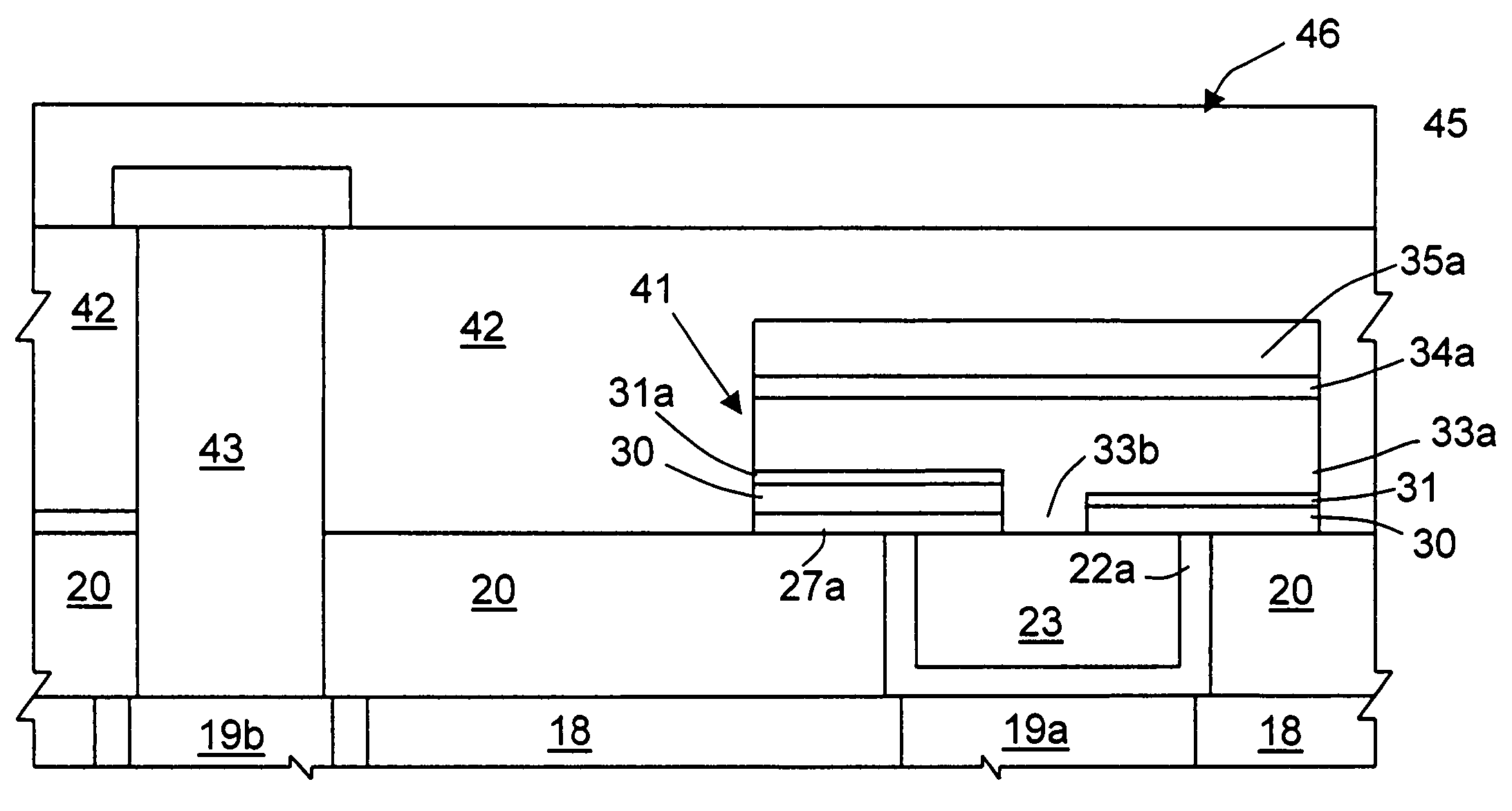
[0028]FIG. 4 illustrates the basic structure of a contact structure according to one embodiment of the invention. In detail, an electronic device 90 has a body 91 (e.g., a substrate) of monocrystalline material defining an upper surface 92 and a lower surface 93 and accommodating electronic components 94, represented schematically. A dielectric layer 95 extends on top of the body 91 and accommodates the contact structure, indicated at 98. The contact structure 98 is formed by a first electrode 100 and an active region 103 of chalcogenic material. The first electrode 100, connected to the electronic components 94 as shown schematically for one of them, has a horizontal portion 102 adjacent to and in contact with the active region 103. A second electrode 104 is formed on the active region 103 and is in electric contact therewith.

[0029]As better shown in the perspective view FIG. 5, the horizontal portion 102 has an elongated shape extending along a longitudinal direction X parallel to...


PUM


Abstract

A contact structure for a PCM device is formed by an elongated formation having a longitudinal extension parallel to the upper surface of the body and an end face extending in a vertical plane. The end face is in contact with a bottom portion of an active region of chalcogenic material so that the dimensions of the contact area defined by the end face are determined by the thickness of the elongated formation and by the width thereof.

Description

BACKGROUND OF THE INVENTION[0001]1. Field of the Invention[0002]The present invention relates to a sub lithographic contact structure, in particular for a phase change memory cell, and a fabrication process thereof.[0003]2. Description of the Related Art[0004]As is known, phase change memory cells utilize a class of materials that have the unique property of being reversibly switchable from one phase to another with measurable distinct electrical properties associated with each phase. For example, these materials may change between an amorphous disordered phase and a crystalline, or polycrystalline, ordered phase. A material property that may change and provide a signature for each phase is the material resistivity, which is considerably different in the two states.[0005]At present, alloys of elements of group VI of the periodic table, such as Te or Se, referred to as chalcogenides or chalcogenic materials, can advantageously be used in phase change cells. The currently most promisi...

Claims


Application Information

Patent Timeline
IPC IPC(8): H01L47/00H01L27/24H01L45/00
CPCH01L27/2445H01L45/06H01L45/122H01L45/126H01L45/1273H01L45/144H01L45/16H10B63/32H10N70/821H10N70/8413H10N70/8418H10N70/231H10N70/011H10N70/8828
Inventor KHOURI, OSAMAPOLLACCIA, GIORGIOPELLIZZER, FABIO
Owner STMICROELECTRONICS SRL
Why Eureka
Try Eureka