Optics landing system and method therefor

a technology of optical landing system and optical element, applied in the field of optical landing system and method therefor, can solve the problems of inability to commercially viable device debugging system by time resolved measurement, inaccessible metal lines, and inability to use fibs, so as to prevent avoid damage to the sil

Inactive Publication Date: 2006-10-17
CREDENCE INC +1
View PDF25 Cites 22 Cited by
  • Summary
  • Abstract
  • Description
  • Claims
  • Application Information

AI Technical Summary

Benefits of technology

[0022]The present invention provides a landing system and method that enables accurate control and placement of the collection optics for a microscope.
[0027]According to a particular feature of the invention, the landing system is further provided with an interrupt to avoid damage to the SIL. The signal from the DVRT is fed to a Schmidt trigger that compares the signal to a preset limit. When that limit is exceeded, an interrupt signal shuts down the stage to prevent damage to the SIL.

Problems solved by technology

One problem in testing flip chips using conventional methods, such as e-beam testing, is that the metal lines are not readily accessible as in other integrated circuits.
However, with the density of today's IC's, the active devices occupy much of the “real estate” available on the substrate, thereby rendering the use of FIB impossible.
However, in spite of the amount of work in the field, there is still no commercially viable system for device debug by time resolved measurements of hot electron emission, as opposed to device illumination.
For example, one of the issues causing difficulties is the efficient collection of the faint light emission.

Method used


Image

  • Optics landing system and method therefor
  • Optics landing system and method therefor
  • Optics landing system and method therefor

Examples


Embodiment Construction

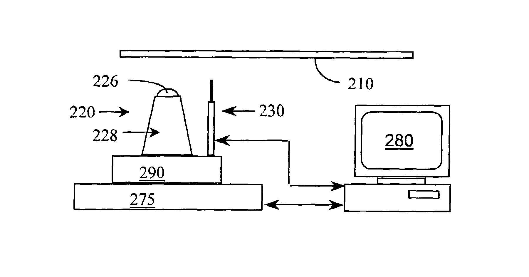
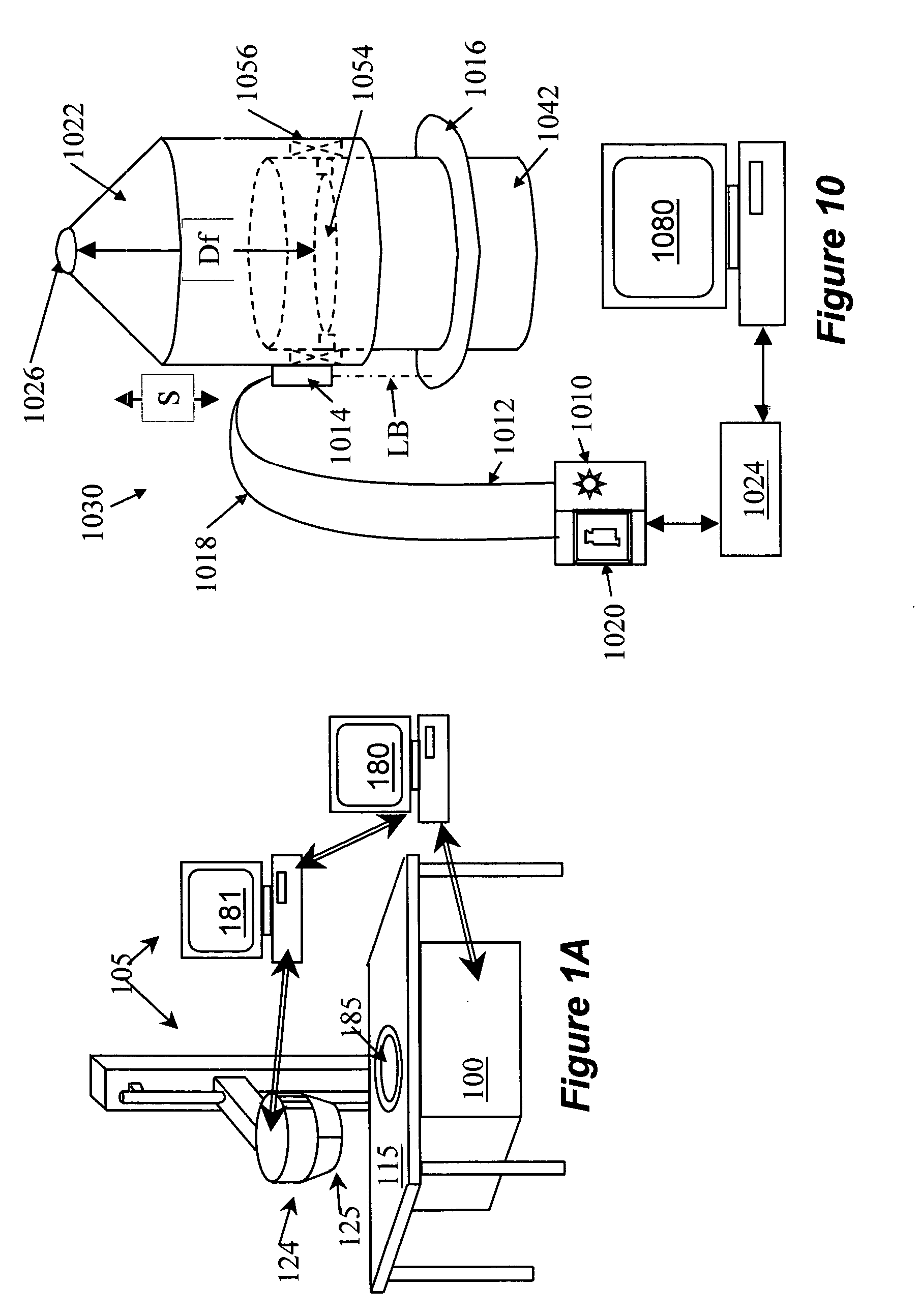
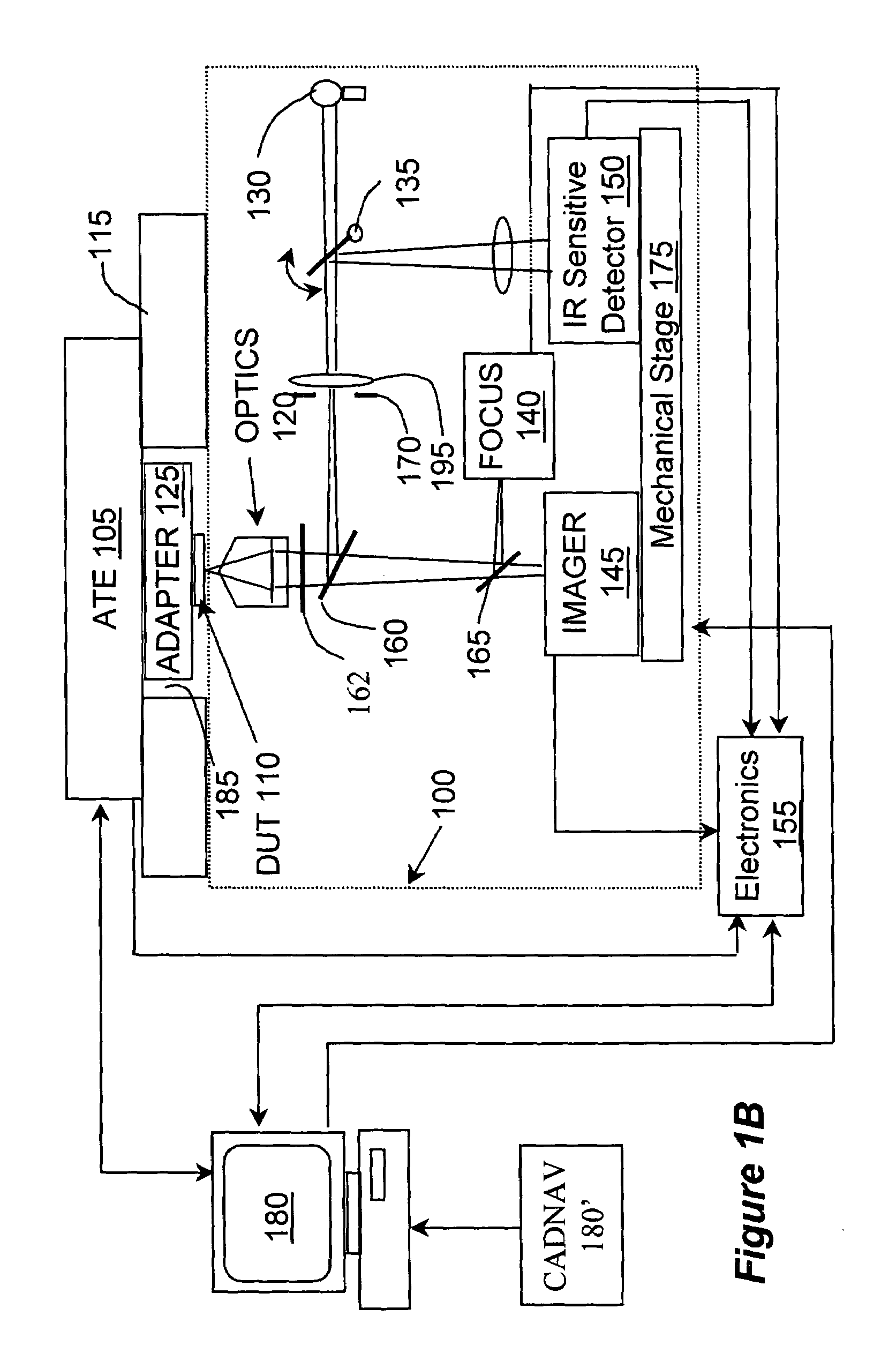
[0040]The present invention provides a landing system for a soft touchdown and accurate placing of collection optics of microscopes. The system can be used with various arrangements of collection optics, and is especially beneficial for use in microscopes designed for detection of faint light emissions. An example of such a microscope is depicted in FIGS. 1A and 1B, illustrating an IC test and debug system. Of course, the inventive landing system is suitable for use with other systems; however, for illustration purposes, various embodiments of the inventive landing system will be described with reference to the test and debug system of FIGS. 1A and 1B.

[0041]FIGS. 1A and 1B are general schematics depicting the major components of the testing and debug system particularly suitable for timing and other testing of microchips, especially from the backside through the substrate (e.g., flip chips). The system operates in conjunction with a commercially available automated testing equipment...


PUM


Abstract

A landing system is provided for accurate placing of collection optics in a microscope. In one example, a solid immersion lens (SIL) is used for light collection, and the landing system is operated to place the SIL in contact with an IC. A proximity sensor is used for determining the SIL's position with respect to the IC. The arrangement is attached to a z-motion stage. During the placement procedure, the navigation is performed in steps and at each step the compression of the SIL is measured relative to its uncompressed state. When a measured compression exceeds a preset threshold, a SIL landing is recognized. In one example, after a landing is recognized, a further compression is imparted to the SIL in order to place the SIL in a focusing distance to the objective lens.

Description

RELATED APPLICATIONS[0001]This application claims priority from, and is a Continuation in Part of, U.S. application Ser. No. 10 / 255,345, filed Sep. 26, 2002, now U.S. Pat. No. 6,828,811, which claims priority from Provisional Application Ser. No. 60 / 371,542, filed Apr. 10, 2002.BACKGROUND OF THE INVENTION[0002]1. Field of the Invention and[0003]The present invention relates to a system for accurate placement of collection optics in microscopes.[0004]2. Description of the Related Art[0005]Various microscopes are used in the art for imaging, testing, and examination of various microstructures. A common feature of these microscopes is that the obtained resolution depends on efficient collection of light from the inspected object. Accurate placing of the collection optics is also highly important for accurate focusing on the object to be inspected. Additionally, to obtain efficient collection of light, the collection optics needs to be accurately placed with respect to the object to be ...

Claims


Application Information

Patent Timeline
Patent Type & Authority Patents(United States)
IPC IPC(8): G01R31/02G01R31/311G02B21/24
CPCG01R31/311G02B21/02G02B21/24
Inventor HANSON, JOHNFRANK, JONATHANMELUZZI, DARIOCOTTON, DANIEL
Owner CREDENCE INC
Why Eureka
Try Eureka