Image sensor with improved uniformity of effective incident light
a technology of effective incident light and image sensor, which is applied in the field of image sensors, can solve the problems of limited fill factor increase and especially problematic phenomenon, and achieve the effect of improving the issue of non-uniform incident ligh
- Summary
- Abstract
- Description
- Claims
- Application Information
AI Technical Summary
Benefits of technology
Problems solved by technology
Method used
Image
Examples
first embodiment
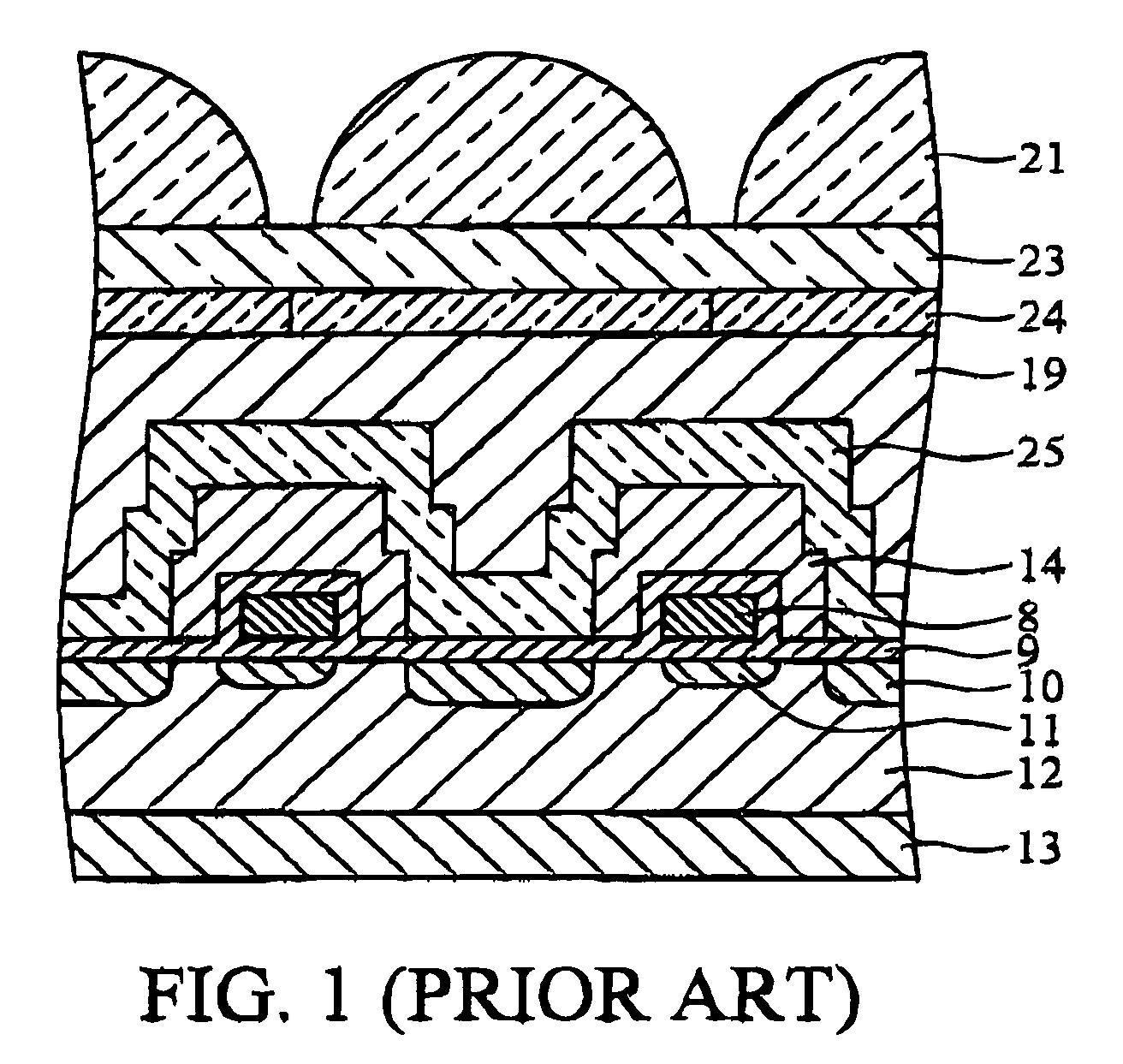
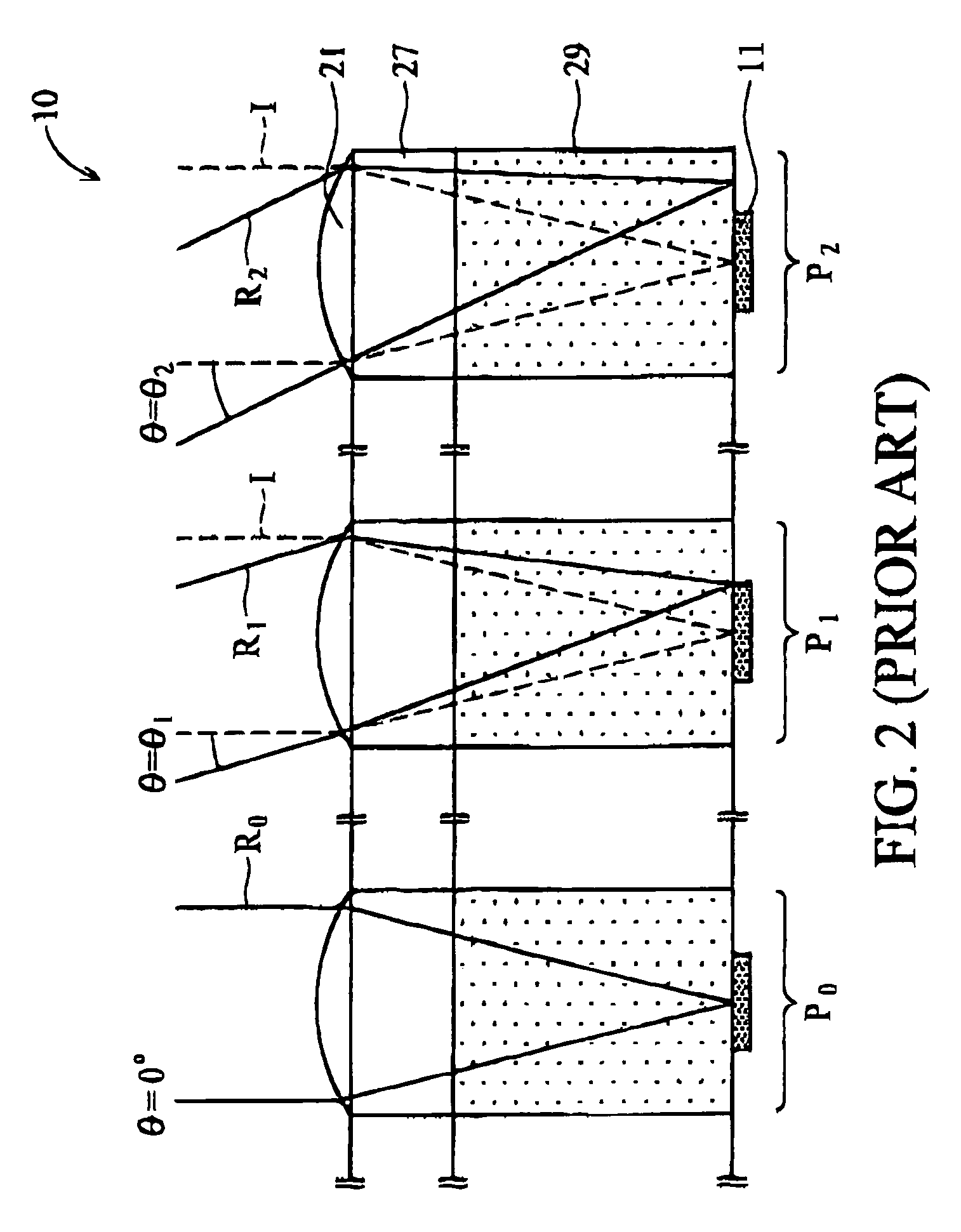
[0022]The incident light transmitted into the microlenses and ranching the sensing areas of an image sensor may not uniformly collimated light, especially for the regions away from the chip center. Therefore the image displayed on the edge region is darker than the center region.
[0023]The present invention provides a method improving the uniformity of effective incident light and avoiding cross-talk between adjacent pixels in a chip equipped with an image sensor so as to balance the brightness in different regions. The microlens layer consists of a plurality of microlenses corresponding to a plurality of sensing areas, respectively. The size of microlens is a function of the distance between microlens to the chip center. Specifically, the size of microlens increases as the distance between the microlens to the chip center increases.
[0024]Progressively increasing the size of the microlenses from the chip center to a chip edge balances the brightness in different regions of the chip. ...
second embodiment
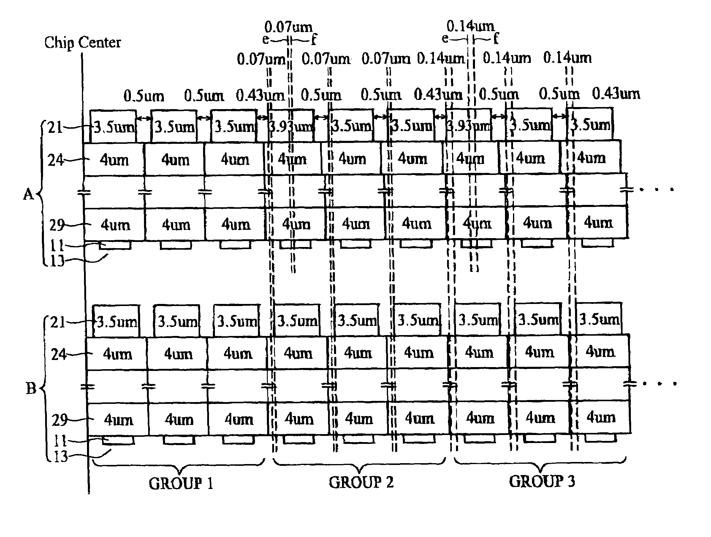
[0029]The present invention provides a method to improve non-uniformly effective incident light and to avoid cross-talk between adjacent pixels in a sensor chip. The microlens layer consists of a plurality of microlenses corresponding to each sensing areas The position of the microlens is a function of distance from the microlens to the chip center. Specitically, the microlens is shifted toward the chip center as the distance between the microlens and the chip center increases. If the microlens is shifted, the corresponding color filter is also shifted to make sure the incident light does not pass through the adjacent color filter.
[0030]A sensor chip with 1284×1028 pixels is given as an example. Each pixel has a width of 4 μm. The chief angle in the edge region furthest away from the chip center is 15° and the furthest microlens needs to be shifted 2.1 μm. The pixels are divided into 31 groups. The relationship between the chief angle and shifting amounts of the microlens and the co...
PUM
 Abstract
Description
Claims
Application Information


