Light-emitting device, image forming apparatus, and display apparatus

a technology of light-emitting devices and image forming devices, which is applied in the direction of static indicating devices, discharge tubes luminescnet screens, instruments, etc., can solve the problems of reducing the brightness of the oled element, difficult to write a voltage signal into the data line at high speed, and producing stray capacitance between, so as to reduce power consumption and prevent brightness from being lowered. , the effect of reducing the stray capacitan

Active Publication Date: 2006-10-24
LUMITEK DISPLAY TECH LTD
View PDF3 Cites 24 Cited by
  • Summary
  • Abstract
  • Description
  • Claims
  • Application Information

AI Technical Summary

Benefits of technology

[0009]An advantage of the invention is that it provides a light-emitting device which is capable of preventing brightness from being lowered and reducing the power consumption by reducing stray capacitance, and an image forming apparatus and a display apparatus using the light-emitting device.
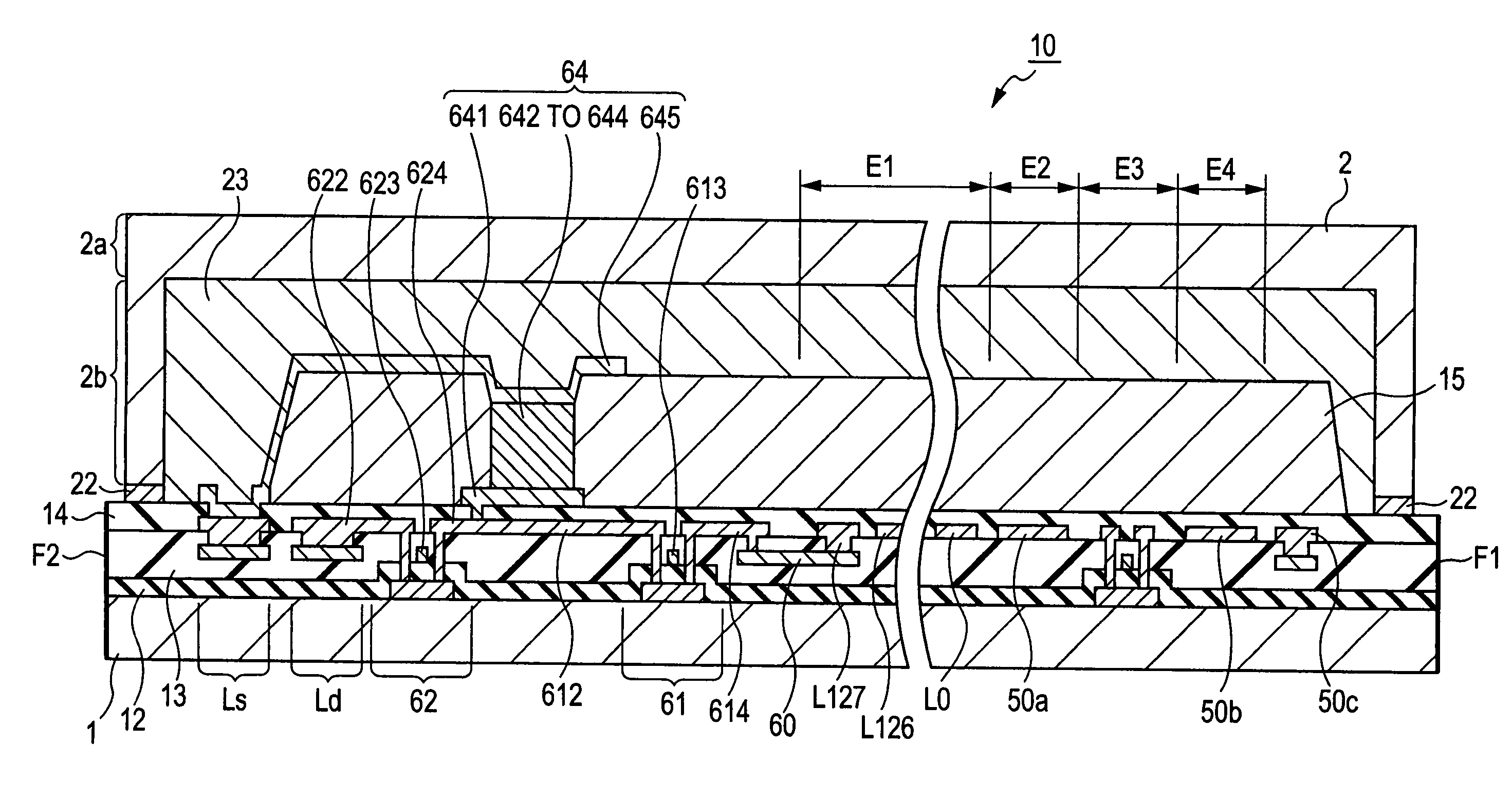
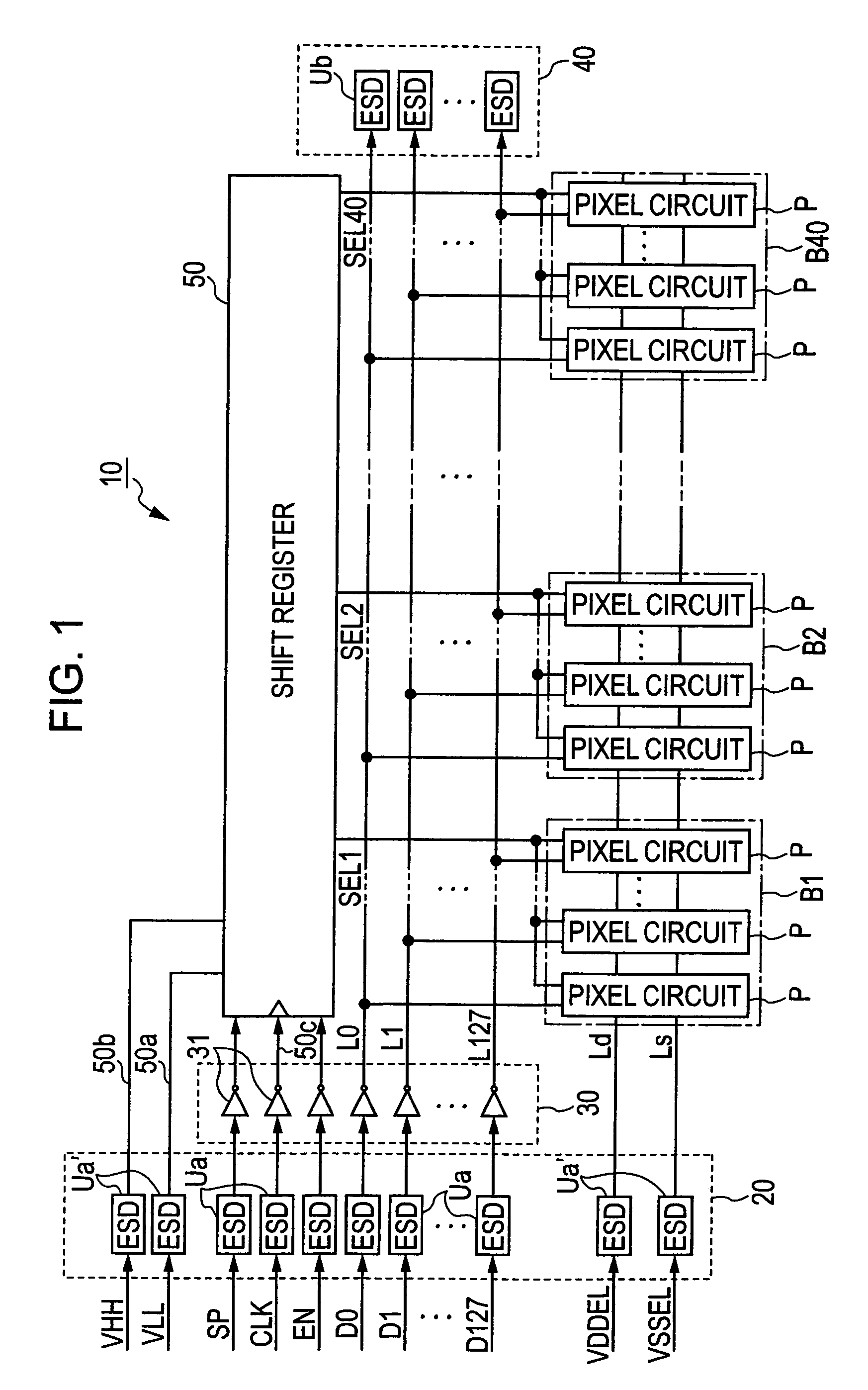
[0010]In order to achieve the above-mentioned object, according to an aspect of the invention, a light-emitting device includes a plurality of data lines, and a plurality of pixel circuits. Each of the plurality of pixel circuits includes a light-emitting element having a first electrode and a second electrode and emitting light having an intensity depending on the amount of driving current, a driving transistor for supplying the driving current to the first electrode, a holding transistor for supplying a driving signal supplied via the data lines to the driving transistor, and a connecting line for connecting the driving transistor to the holding transistor. The second electrode is formed in a region different from a region in which the data lines are formed such that the second electrode is not opposite to some or all of the data lines.
[0011]According to this invention, since the second electrode of the light-emitting element is not opposite to some or all of the data lines, a stray capacitance occurring between the second electrode and the data lines can be reduced. As a result, since a voltage of the data lines can be easily changed to have large amplitude, the brightness of the light-emitting element can be enhanced. In addition, since the capacitive load can be reduced, a driving circuit with low driving capability can be used and it becomes possible to reduce power consumption. In addition, from a point of view of the reduction of the stray capacitance, it is preferable to form the second electrode in a region different from a region in which the data lines are formed such that the second electrode is not opposite to all of the data lines. The light-emitting device is manufactured by forming a semiconductor layer, an interlayer insulating layer, electrodes, wiring lines and the like on a substrate. Accordingly, the data lines do not occupy the same region as the second electrode. Here, the term ‘region’ means a range in which objects (the second electrode and the data lines) are formed on the light-emitting device in plan view, for example, when reviewed in a direction perpendicular to the second electrode in plan view.
[0012]Particularly, if the second electrode is formed in a region different from a region in which the data lines are formed such that the second electrode is not opposite to all of the data lines, it is very suitable to an image forming apparatus in which the light-emitting device is used as a line head. On the other hand, if the second electrode is formed in a region different from a region in which the data lines are formed such that the second electrode is not opposite to some of the data lines, it is suitable to a display apparatus using the light-emitting device. In the display apparatus, pixel circuits are arranged in the form of a matrix at intersections of the plurality of scanning lines and a plurality of data lines. From a point of view of uniformity of brightness on the entire screen, potentials of cathodes of the pixel circuits are preferably maintained constant. To this end, second electrodes are connected one another to lower the total impedance. However, if the second electrode are arranged to cover the data lines, the stray capacitance occurs. So, it is preferable to form the second electrode such that it is not opposite to some of the data lines.
[0013]According to another aspect of the invention, a light-emitting device includes a plurality of data lines, and a plurality of pixel circuits. Each of the plurality of pixel circuits includes a light-emitting element having a first electrode and a second electrode and emitting light having an intensity depending on the amount of driving current, a driving transistor for supplying the driving current to the first electrode, a holding transistor for supplying a driving signal supplied via the data lines to the driving transistor, and a connecting line for connecting the driving transistor to the holding transistor. The second electrode is formed in a region different from a region in which the holding transistor is formed such that the second electrode is not opposite to the holding transistor.
[0014]According to this invention, since the second electrode of the light-emitting element is not opposite to some or all of the holding transistor, a stray capacitance occurring between the second electrode and the data lines can be reduced. As a result, since a voltage of the data lines can be easily changed to have large amplitude, the brightness of the light-emitting element can be enhanced. In addition, since the capacitive load can be reduced, a driving circuit with low driving capability can be used and it becomes possible to reduce power consumption.

Problems solved by technology

However, when the cathode is opposite to the data line, a stray capacitance is produced between the cathode and the data line.
Accordingly, if the driving circuit has low driving capability, there is a problem in that it is difficult to write a voltage signal into the data line at high speed, and the brightness of the OLED element is lowered.
On the other hand, even if a driving circuit having high driving capability is used a high load still needs to be driven and therefore, there is a problem in that power consumption is increased.
In addition, since the stray capacitance is increased when the holding transistor is opposite to the cathode of the OLED element, there is the same problem as in the data line.
Particularly, when an operation state of the driving transistor is controlled by supplying a driving signal having a preset pulse width to the driving transistor and the brightness of the OLED element is controlled by the preset pulse width, there arises a problem in that the driving signal having the preset pulse width is deteriorated due to the capacitive load, and thus, the desired brightness may not be obtained.
More particularly, when the light-emitting device is applied to a head unit of an image forming apparatus, since the OLED element is required to have high brightness because of sensitivity of a photoreceptor, there arises a significant problem of lack of write due to the stray capacitance.
In addition, if the write period in a large display panel is short, there is also a significant problem of lack of write due to the stray capacitance.
However, if the second electrode are arranged to cover the data lines, the stray capacitance occurs.
In general, performance of the light-emitting element is deteriorated when it is exposed to oxygen.
However, in any case, actually, external gases intrude into the sealing structure.

Method used


Image

  • Light-emitting device, image forming apparatus, and display apparatus
  • Light-emitting device, image forming apparatus, and display apparatus
  • Light-emitting device, image forming apparatus, and display apparatus

Examples


Embodiment Construction

[0043]Hereinafter, exemplary embodiments of the present invention will be described with reference to the accompanying drawings.

Light-Emitting Device

[0044]FIG. 1 is a block diagram illustrating the configuration of a light-emitting device according to an embodiment of the invention. The light-emitting device is used as a head unit 10 of an image forming apparatus, such as a printer. The head unit 10 is a line-type optical head and includes an input protection circuit 20, a buffer unit 30, 128 data lines L0 to L127, an output protection circuit 40, a shift register 50, and a plurality of pixel blocks B1 to B40. The head unit 10 is supplied with various control signals and power signals in addition to data signals D0 to D127, and the input protection circuit 20 includes a plurality of input ESD protection units Ua arranged on wiring lines for supplying the control signals, and a plurality of inter-power protection unit Ua′ arranged between a plurality of power supplies for supplying p...


PUM


Abstract

A light-emitting device has a plurality of data lines and a plurality of pixel circuits. Each of the plurality of pixel circuits includes a light-emitting element that has a first electrode and a second electrode and that emits light having an intensity depending on the amount of driving current; a driving transistor that supplies the driving current to the first electrode; a holding transistor that supplies a driving signal supplied via the data lines to the driving transistor; and a connecting line that connects the driving transistor to the holding transistor. The second electrode is formed in a region different from a region in which the data lines are formed such that the second electrode is not opposite to some or all of the data lines.

Description

BACKGROUND OF THE INVENTION[0001]1. Technical Field[0002]The present invention relates to a light-emitting device using light-emitting elements for emitting light having an intensity depending on the amount of current flowing from an anode to a cathode, such as an organic light-emitting diode element, to an image forming apparatus, and to a display apparatus.[0003]2. Related Art[0004]In recent years, a great deal of attention has been paid to organic electroluminescent elements or organic light-emitting diode (OLED) elements, which are also called light-emitting polymer elements, as next-generation light-emitting devices replacing liquid crystal devices. Since the OLED element is a self-emitting type, a panel using the OLED element has a low dependency on a viewing angle, and moreover, since the OLED element does not require a backlight or reflected light, this element is suitable for a thin display device with low power consumption.[0005]The OLED element is a current driven element...

Claims


Application Information

Patent Timeline
Patent Type & Authority Patents(United States)
IPC IPC(8): H01J1/62
CPCH01L27/3244H01L51/5221G09G3/3225G09G3/3291G09G2300/0426G09G2300/0439G09G2300/0847G09G2320/0223G09G2330/021H01L27/3276H10K59/12H10K59/131H10K50/82G09G3/30G03G15/02G03G15/04
Inventor KITAZAWA, TAKAYUKI
Owner LUMITEK DISPLAY TECH LTD
Why Eureka
Try Eureka