Means scanning scan path parts sequentially and capturing response simultaneously

a scanning path and sequential technology, applied in the direction of resistance/reactance/impedence, testing circuits, instruments, etc., can solve the problems of increasing the cost of manufacturing ic, lengthening the test time, and adding undesirable delays, so as to reduce the test power consumption, reduce the test time, and reduce the test time

Inactive Publication Date: 2006-10-31
TEXAS INSTR INC
View PDF4 Cites 5 Cited by
  • Summary
  • Abstract
  • Description
  • Claims
  • Application Information

AI Technical Summary

Benefits of technology

[0016]The present invention describes a method of adapting conventional scan architectures into a low power scan architecture. The low power scan architecture maintains the test time of conventional scan architectures, while requiring significantly less operational power than conventional scan architectures. The low power scan architecture is advantageous to IC / die manufacturers since it allows a larger number of circuits (such as DSP or CPU core circuits) embedded in an IC / die to be tested in parallel without consuming too much power within the IC / die. Since the low power scan architecture reduces test power consumption, it is possible to simultaneously test more die on a wafer than previously possible using conventional scan architectures. This allows wafer test times to be reduced which reduces the manufacturing cost of each die on the wafer.

Problems solved by technology

This lengthens the test time of the IC, which increases the cost to manufacture the IC.
The problem with the first method is that it adds an undesirable delay (i.e. the blocking circuit delay) in the stimulus paths 216 between D-FFs 204 and logic 108.
This delay can negatively effect the performance of circuit 100 when it is configured into its normal functional mode.
The problem with the second method is that it increases the test time since scan operations are performed at the reduced scan clock rate.

Method used


Image

  • Means scanning scan path parts sequentially and capturing response simultaneously
  • Means scanning scan path parts sequentially and capturing response simultaneously
  • Means scanning scan path parts sequentially and capturing response simultaneously

Examples


Embodiment Construction

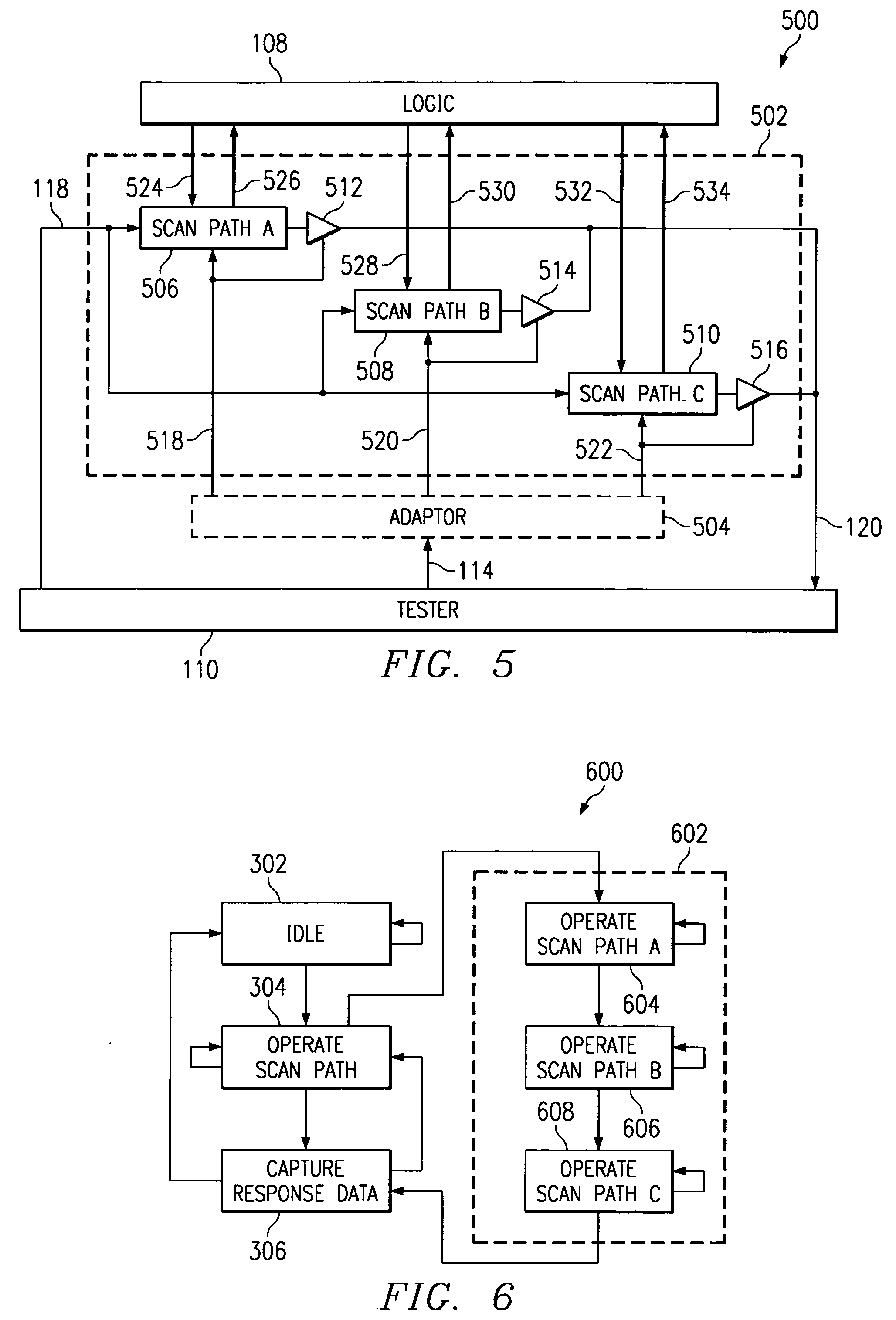
[0039]FIG. 5 illustrates the scan architecture of FIG. 1 after it has been adapted into the low power scan architecture of the present invention. The changes between the FIG. 1 scan architecture and the FIG. 5 low power scan architecture involve modification of scan path 104 into scan path 502, and the insertion of an adaptor circuit 504 in the control path 114 between tester 110 and scan path 502.

[0040]Adapting scan path 104 into scan path 502 involves reorganizing scan path 104 from being a single scan path containing all the scan cells (M), into a scan path having a desired number of selectable separate scan paths. In FIG. 5, scan path 502 is shown after having been reorganized into three separate scan paths A 506, B 508, and C 510. It is assumed at this point in the description that the number of scan cells (M) in scan path 104 is divisible by three such that each of the three separate scan paths A, B, and C contains an equal number of scan cells (M / 3). The case where scan path ...


PUM


Abstract

Scan architectures are commonly used to test digital circuitry in integrated circuits. The present invention describes a method of adapting conventional scan architectures into a low power scan architecture. The low power scan architecture maintains the test time of conventional scan architectures, while requiring significantly less operational power than conventional scan architectures. The low power scan architecture is advantageous to IC/die manufacturers since it allows a larger number of circuits (such as DSP or CPU core circuits) embedded in an IC/die to be tested in parallel without consuming too much power within the IC/die. Since the low power scan architecture reduces test power consumption, it is possible to simultaneously test more die on a wafer than previously possible using conventional scan architectures. This allows wafer test times to be reduced which reduces the manufacturing cost of each die on the wafer.

Description

CROSS-REFERENCE AND INCORPORATION BY REFERENCE OF RELATED APPLICATION[0001]This application is a divisional of application Ser. No. 09 / 803,599, filed Mar. 9, 2001 now U.S. Pat No. 6,769,080, and claims priority from Provisional Application No. 60 / 187,972, filed Mar. 9, 2000. This disclosure relates to and incorporates by reference application Ser. No. 09 / 339,734, now U.S. Pat. No. 6,519,729, Application Ser. No. 60 / 188,109, now U.S. Pat. No. 6,763,488.BACKGROUND OF THE INVENTION[0002]1. Field of the Invention[0003]Scan architectures are commonly used to test digital circuitry in integrated circuits. The present invention describes a method of adapting conventional scan architectures into a low power scan architecture. The low power scan architecture maintains the test time of conventional scan architectures, while requiring significantly less operational power than conventional scan architectures. The low power scan architecture is advantageous to IC / die manufacturers since it allow...

Claims


Application Information

Patent Timeline
Patent Type & Authority Patents(United States)
IPC IPC(8): G01R31/28G01R31/317G01R31/3185
CPCG01R31/31721G01R31/318536G01R31/318575G01R31/318577G01R31/3177G01R31/31723
Inventor WHETSEL, LEE D.
Owner TEXAS INSTR INC
Why Eureka
Try Eureka