Circuit device and method of measuring clock jitter

a clock jitter and circuit device technology, applied in the direction of noise figure or signal-to-noise ratio measurement, resistance/reactance/impedence, instruments, etc., can solve the problem of difficult to accurately measure the reduction of processor frequency, the parametric yield limitation of the clock jitter circuit device, and the difficulty of reducing the processor frequency. problem, to achieve the effect of enhancing the operating clock speed of the circuit device, reducing the clock jitter margin, and high accuracy in

Active Publication Date: 2010-10-19
QUALCOMM INC
View PDF27 Cites 12 Cited by
  • Summary
  • Abstract
  • Description
  • Claims
  • Application Information

AI Technical Summary

Benefits of technology

[0011]One particular advantage provided by embodiments of the clock jitter determination circuit is provided in that the clock jitter determination circuit achieves high accuracy in determining clock jitter, allowing designers to set a smaller clock jitter margin to enhance operating clock speeds for circuit devices.
[0012]Another particular advantage is provided in that the clock jitter determination circuit occupies a smaller area of the overall circuit and consumes less operating power than jitter compensation circuits and / or conventional clock jitter determination circuits.
[0013]Yet another particular advantage is provided in that the clock jitter determination circuit is adapted to measure jitter over long periods of time on processor cores that are executing various applications.
[0014]Another particular advantage is provided in that the clock jitter determination circuit can operate without calibration.

Problems solved by technology

Short-term clock fluctuations, or clock jitter, can degrade system performance due to a hazard of timing constraint violations.
Clock jitter introduces a parametric yield limitation in circuit devices, because the clock jitter affects the maximum frequency at which core processors can operate.
Conventionally, a reduction in the processor frequency can be difficult to measure accurately, in part, because insertion of measurement points may also perturb the clock signal.
For example, external test probes measuring clock jitter may perturb the clock signal by introducing capacitances, inductances, impedance mismatches, and other anomalies that can introduce additional clock fluctuations.
However, to accurately sample the clock signal, a large number of sampling points and therefore a large number of flip-flops are used.
The large number of flip-flops can occupy significant area of the overall circuit.
Further, accuracy associated with such test structures is typically limited to the insertion delay of each element of the delay chain.
This operating margin limits the frequency at which the circuit device can operate.
Further, once clock jitter in a particular circuit design is measured, it remains difficult to determine whether a design change may reduce jitter.
While an excessive jitter margin may increase area usage of a circuit substrate, increase power consumption, and increase a time to market for a particular design, an insufficient jitter margin may result in reduced quality and increased number of failures or reduced yield.

Method used


Image

  • Circuit device and method of measuring clock jitter
  • Circuit device and method of measuring clock jitter
  • Circuit device and method of measuring clock jitter

Examples


Embodiment Construction

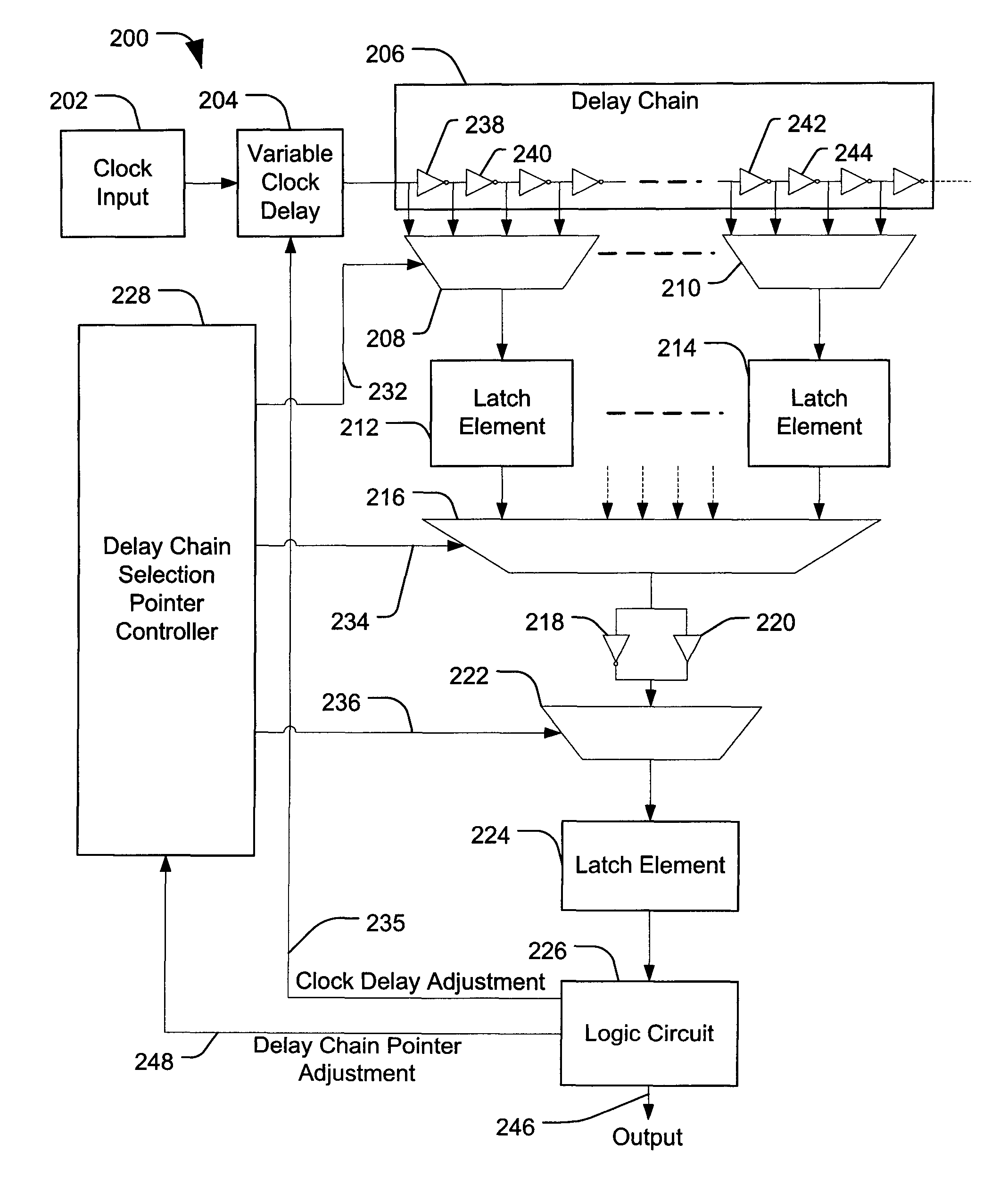
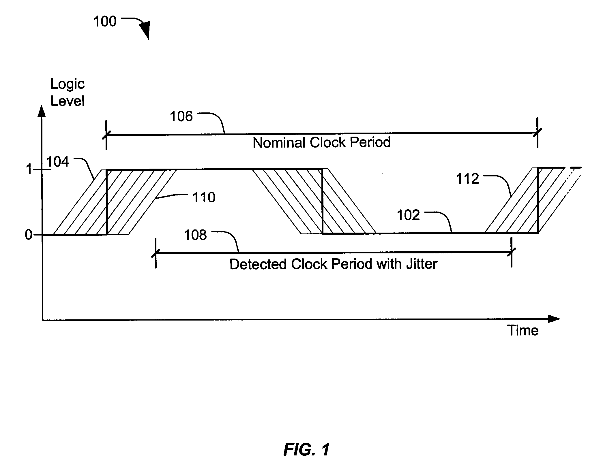
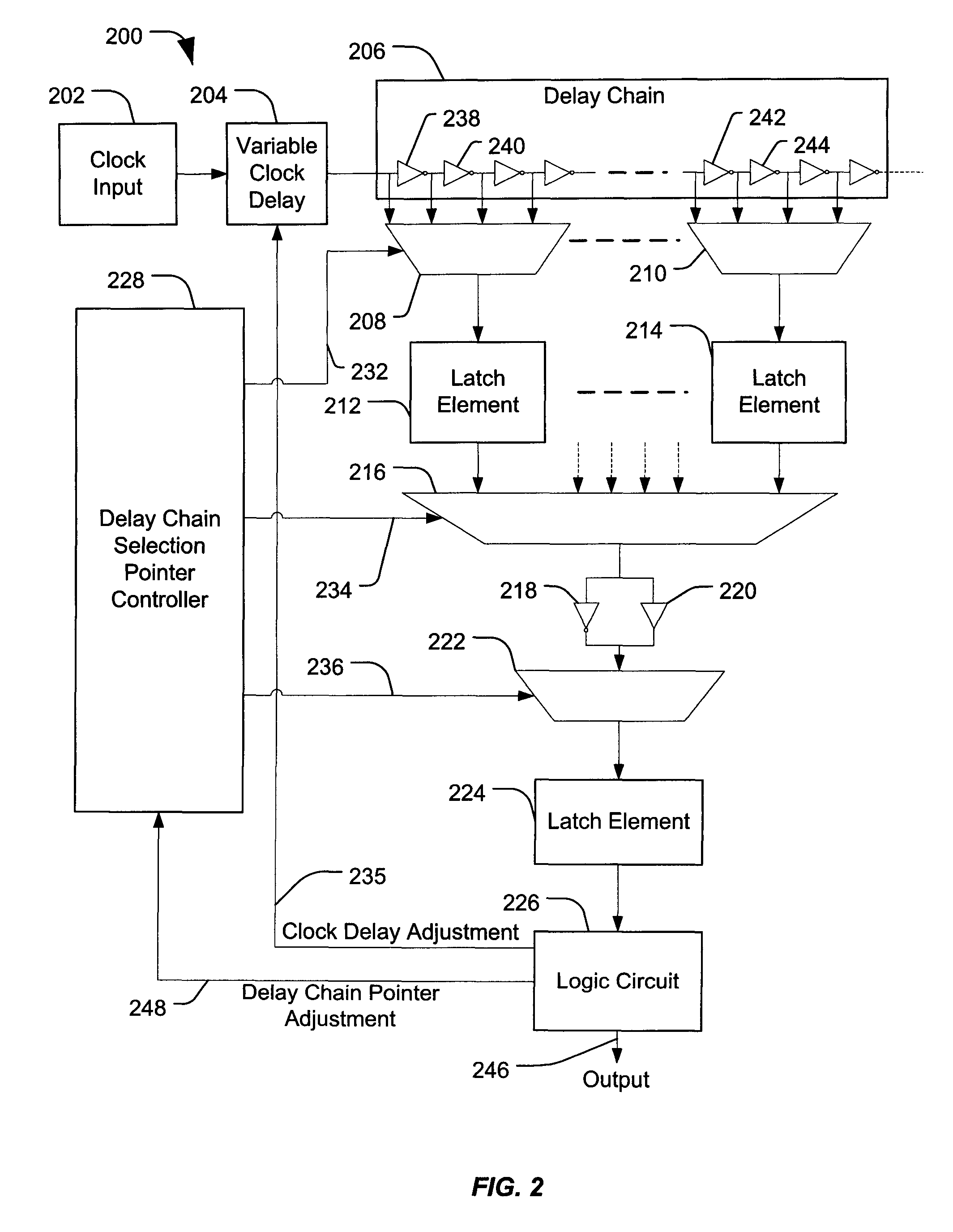
[0025]FIG. 1 is a graph 100 illustrating a clock signal 102 that includes timing uncertainty due to jitter. The graph 100 includes an x-axis representing time and a y-axis representing a logic level or voltage level. It should be understood that the time axis may indicate time in units of circuit delay, units of absolute time (such as nanoseconds), other units, or any combination thereof. The clock signal 102 has a nominal clock period 106 and has a detected clock period with jitter 108. In general, clock jitter is a distortion in clock cycle and phase difference accumulated over time, such that the clock edge (rising edge, falling edge or both) may be distorted, or may arrive early or late relative to an expected nominal clock edge. Early rising clock edges caused by jitter are generally indicated by reference numerals 104 and 112 and a delayed clock edge is generally indicated by reference numeral 110.

[0026]In general, the clock signal 102 may include multiple potential transition...


PUM


Abstract

In an embodiment, a method is disclosed that includes receiving a clock signal at a delay chain of a circuit device and determining a value of the clock signal at a selected point within the delay chain. The method also includes adjusting the selected point when the value does not indicate detection of an edge of the clock signal.

Description

BACKGROUND[0001]I. Field[0002]The present disclosure is generally related to circuit devices and methods of measuring clock jitter.[0003]II. Description of Related Art[0004]In general, the temporal stability of a clock signal within a circuit device can impact performance, particularly within synchronous digital circuit devices. Short-term clock fluctuations, or clock jitter, can degrade system performance due to a hazard of timing constraint violations. Clock jitter introduces a parametric yield limitation in circuit devices, because the clock jitter affects the maximum frequency at which core processors can operate. Conventionally, a reduction in the processor frequency can be difficult to measure accurately, in part, because insertion of measurement points may also perturb the clock signal. For example, external test probes measuring clock jitter may perturb the clock signal by introducing capacitances, inductances, impedance mismatches, and other anomalies that can introduce add...

Claims


Application Information

Patent Timeline
Patent Type & Authority Patents(United States)
IPC IPC(8): H03L7/06
CPCH03L7/00G04F10/005G01R29/26G01R31/31709
Inventor SAINT-LAURENT, MARTINANDREEV, BORIS DIMITROVBASSETT, PAUL
Owner QUALCOMM INC
Why Eureka
Try Eureka