

Optimal bank shapes for inkjet printing
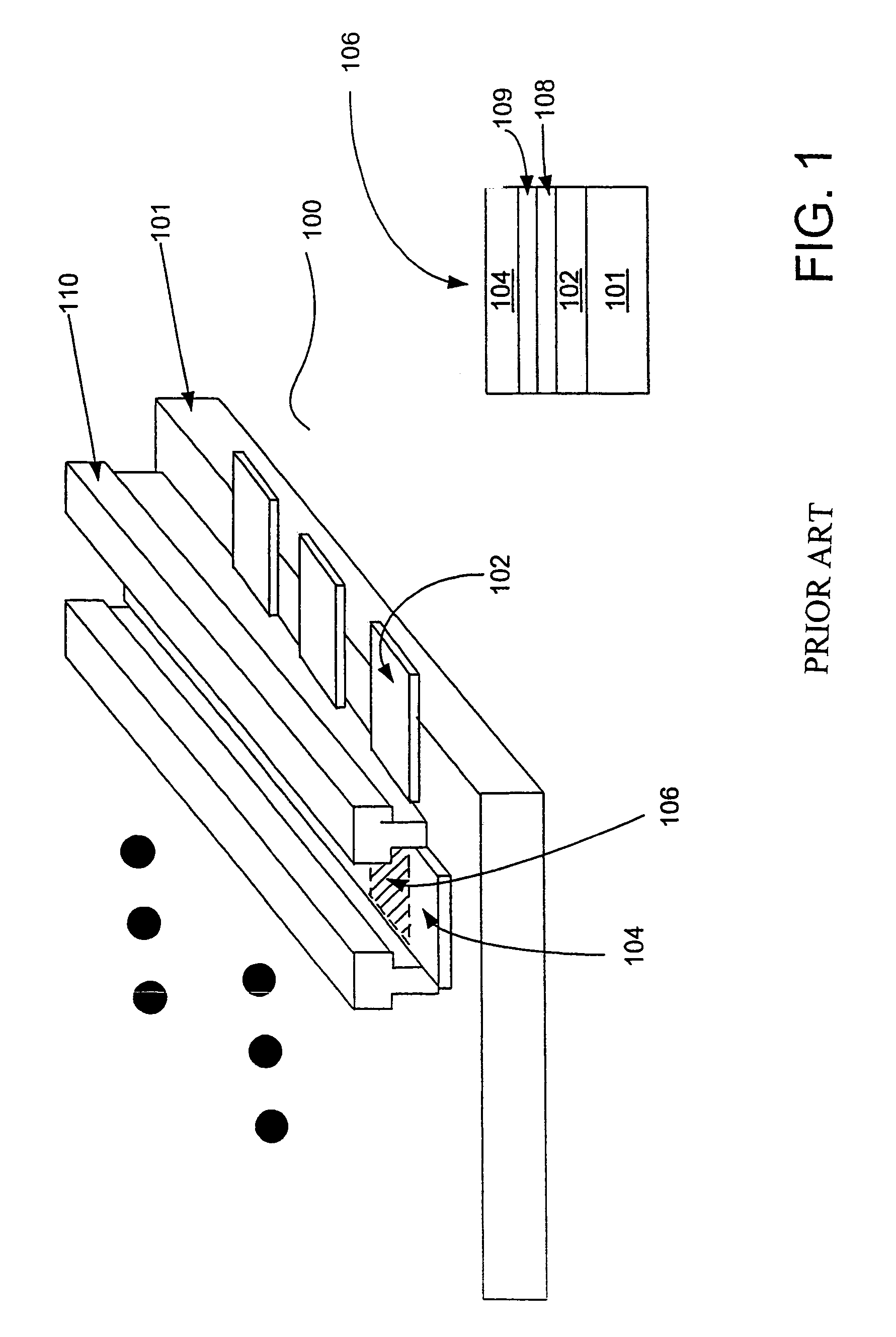
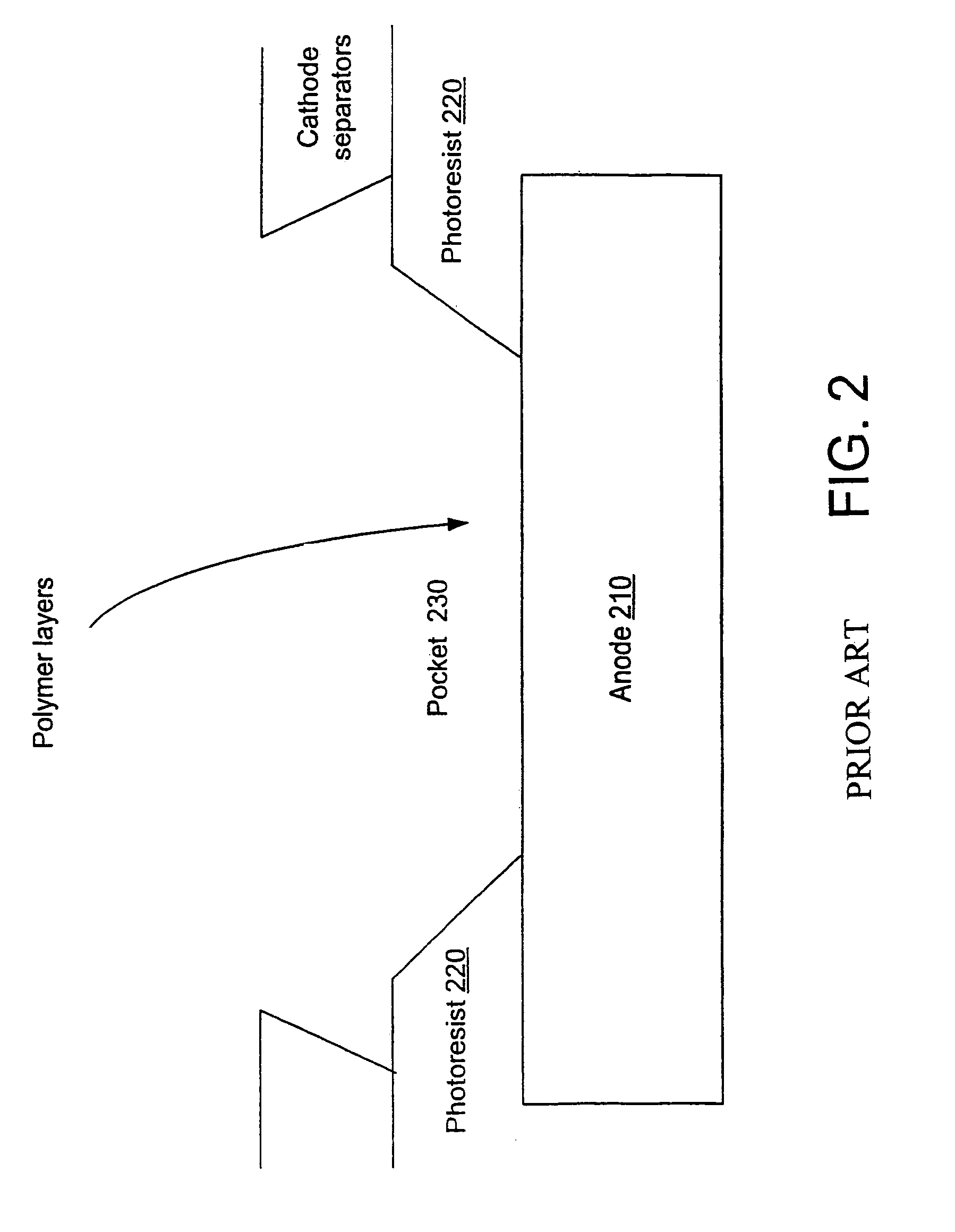
a technology of inkjet printing and bank shape, which is applied in the manufacture of electrode systems, electric discharge tubes/lamps, discharge tubes luminescnet screens, etc., can solve the problems of uniform and concave drying patterns, affecting the spread/flow/shape of deposited polymers of cathode separators, and reducing the level of build-up of inkjet printing, so as to reduce the level of build-up, uniform and flatter profile, and uniform drying profiles profil
- Summary
- Abstract
- Description
- Claims
- Application Information
AI Technical Summary
Benefits of technology
Problems solved by technology
Method used
Image

Examples
Embodiment Construction
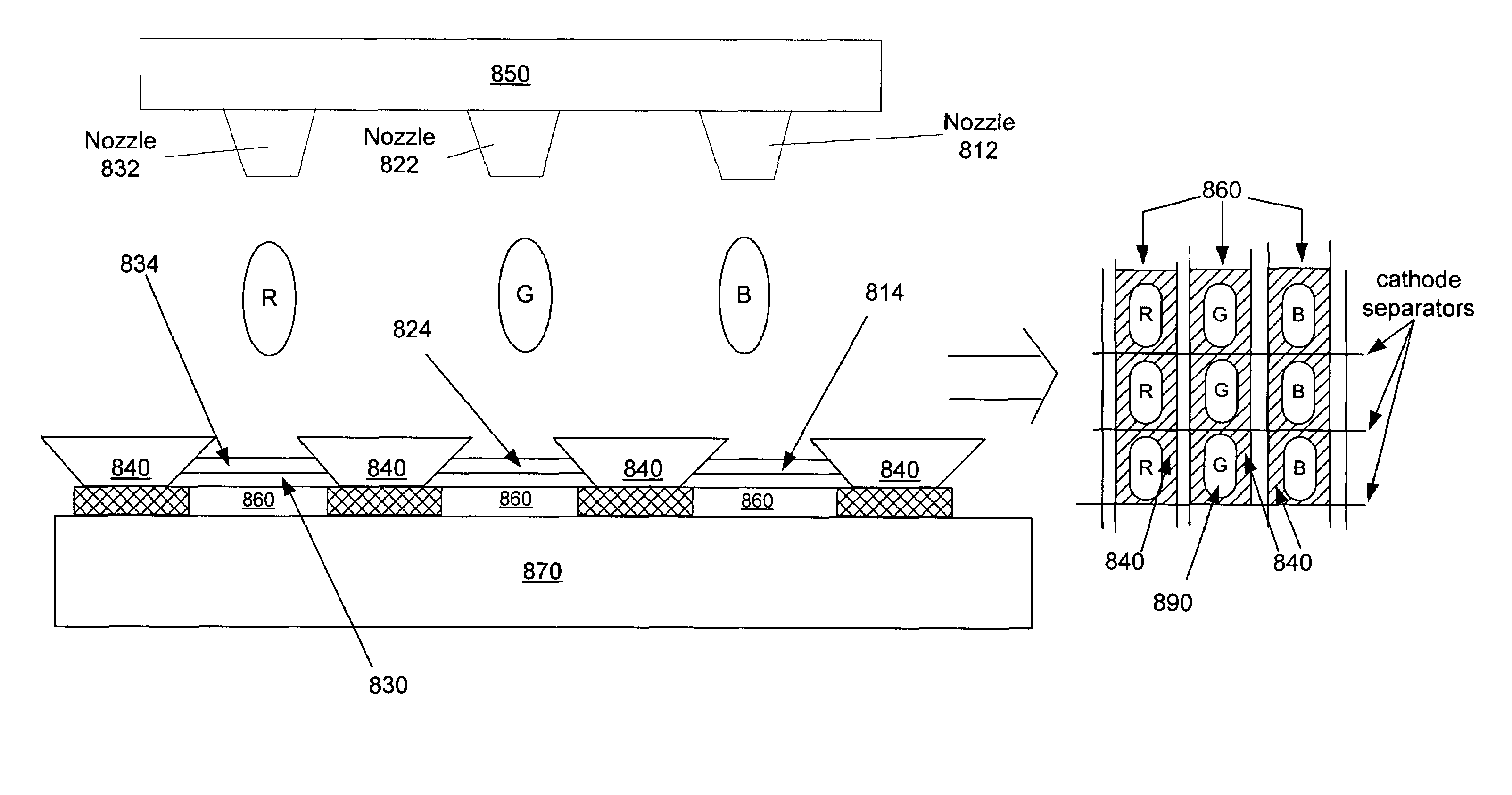
[0030]In accordance with the invention, the shapes of the photo-resist layer “banks” which define pockets for inkjet printing or other patterned processes are optimized to provide a more uniform drying profile for substances which are to be deposited in those pockets. Preferably, the shapes of the banks are such that a portion of the photo-resist layer overhangs the exposed lower electrode layer. Due to this overhang feature, such banks are referred to as “mushroom” (or “undercut”) banks. In one embodiment of the invention, the banks are trapezoidal in configuration such that the angle between the side wall of the photo-resist bank and the edge of the lower electrode layer which the side wall contacts is less than or equal to ninety degrees. This configuration may be exhibited on any or all of the four bank walls which define a pocket. This configuration reduces the level of build-up on and near the walls of the banks and induces a more uniform and flatter profile when a substance d...
PUM
 Abstract
Description
Claims
Application Information