Method of electrical testing

a technology of electrical testing and device, applied in the field of device fabrication, can solve the problems of affecting the test throughput, and affecting the test accuracy of the device,

Inactive Publication Date: 2006-11-07
BELL SEMICON LLC
View PDF9 Cites 2 Cited by
  • Summary
  • Abstract
  • Description
  • Claims
  • Application Information

AI Technical Summary

Problems solved by technology

Normally, after only a few touchdowns, the contact resistance between the probe and the bump increases significantly and is very unstable, resulting in erroneous electrical measurements.
A similar problem may exist even without solder when aluminum pads are used, since aluminum oxide tends to build up on the probes.
This process can be time consuming.
In fact, cleaning is required so often that the test throughput is severely curtailed.
Also, the probe card wears out more quickly resulting in a higher cost for the tests.

Method used


Image

  • Method of electrical testing
  • Method of electrical testing

Examples


Embodiment Construction

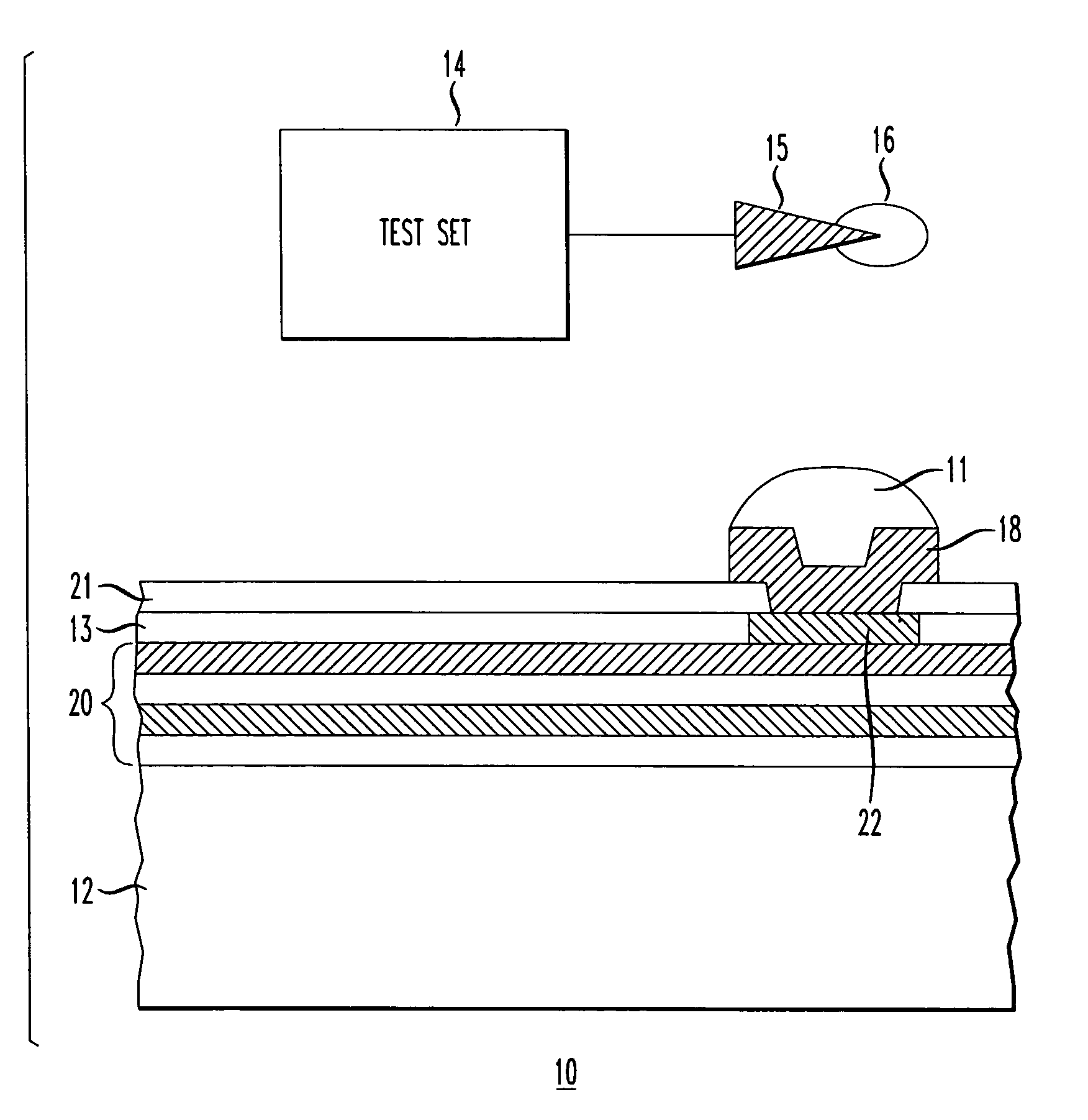
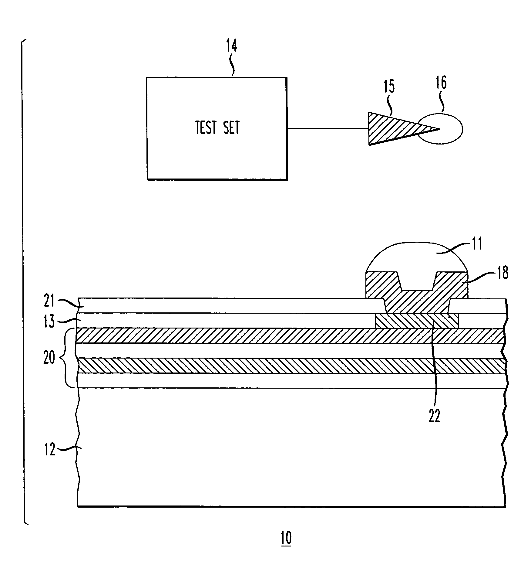
[0010]Referring now to the drawing, the FIGURE is a schematic cross sectional view of a portion of an integrated circuit chip, 10, during a testing phase in the fabrication of the circuit. The chip includes the standard topological features such as alternate layers of dielectric and conductive layers, 20, formed over the semiconductor substrate, 12. Planarization layers, 13 and 21, are typically formed over essentially the entire surface of the chip. In this example, the substrate, 12, was silicon, and the planarization layers, 13 and 21, were polyimide and silicon nitride formed by standard techniques such as plasma enhanced chemical vapor deposition. The chip also includes metal areas, e.g., 22, on the surface through which electrically conductive bonding pads, e.g., 18, provide electrical contact to the underlying conductive layers.

[0011]A solder bump, 11, is formed on the pad, 18, by standard techniques. In a preferred embodiment, the solder was a lead-free solder which is parti...


PUM

PropertyMeasurementUnit
electrically testingaaaaaaaaaa
resistivityaaaaaaaaaa
viscosityaaaaaaaaaa

Abstract

A method of electrical testing devices such as integrated circuits that include conductive pads formed on the surface. A material having a desired bulk resistivity and viscosity is applied to either the device or the electrical probe prior to testing. The application of the material has been found to substantially reduce the need for cleaning of the probe.

Description

CROSS REFERENCE TO RELATED APPLICATION [0001]This application claims the benefit of co-pending provisional application No. 60 / 592,153, filed Jul. 29, 2004.FIELD OF THE INVENTION [0002]The present invention relates generally to the fabrication of devices and, more particularly, to a method of electrically probing the devices.BACKGROUND OF THE INVENTION [0003]During the fabrication of semiconductor integrated circuits and other devices, it is often desirable to apply an electrical probe to the contact pads of the chip in order to test the circuit. This probing is preferably done after solder bumps have been formed on the pads in order to prevent damage to the pads that can result in leakage. Normally, after only a few touchdowns, the contact resistance between the probe and the bump increases significantly and is very unstable, resulting in erroneous electrical measurements. A similar problem may exist even without solder when aluminum pads are used, since aluminum oxide tends to buil...

Claims


Application Information

Patent Timeline
Patent Type & Authority Patents(United States)
IPC IPC(8): G01R31/02C23C16/52C23C20/00
CPCG01R1/06783G01R31/2884G01R31/2886
Inventor GOLDEN, JAMESRADEMACHER, WAYNESCHUMACHER, CALVIN LEESEITZER, PHILIP WILLIAMSTANG, STEVEN V.
Owner BELL SEMICON LLC
Why Eureka
Try Eureka