Connector circuit board

a technology of connecting circuit board and connector, which is applied in the direction of measuring leads/probes, coupling device connections, instruments, etc., can solve the problems of high cost of electrical connection, high cost of jig bearing spring probes, and high cost of parts of connectors, so as to achieve easy and reliable electrical connection and low cost

Inactive Publication Date: 2006-11-14
FUJITSU LTD
View PDF9 Cites 20 Cited by
  • Summary
  • Abstract
  • Description
  • Claims
  • Application Information

AI Technical Summary

Benefits of technology

[0007]An object of the present invention is to provide a connector which can connect a test device to a printed circuit board at a relatively low cost.
[0012]According to the present invention, a connector can be relatively easily and reliably electrically connected to a printed circuit board by touching conducting pins to electrode pads. Moreover, when a fixing pin is fitted into a fixing hole, the electrical connection of the conducting pins to the electrode pads is ensured. If the connector is connected to a test device, the test device and the printed circuit board are connected to each other at a relatively low cost.

Problems solved by technology

This method makes it necessary to develop and manufacture jigs in line with printed circuit boards, and the cost of development and manufacture of a jig arises for each type of printed circuit board.
Moreover, the jig bearing the spring probes has a relatively complex structure and a mechanism for supporting the printed circuit board is needed.
The expenses of parts of a connector and the labor and cost for mounting the connector arise.

Method used


Image

  • Connector circuit board
  • Connector circuit board
  • Connector circuit board

Examples


Embodiment Construction

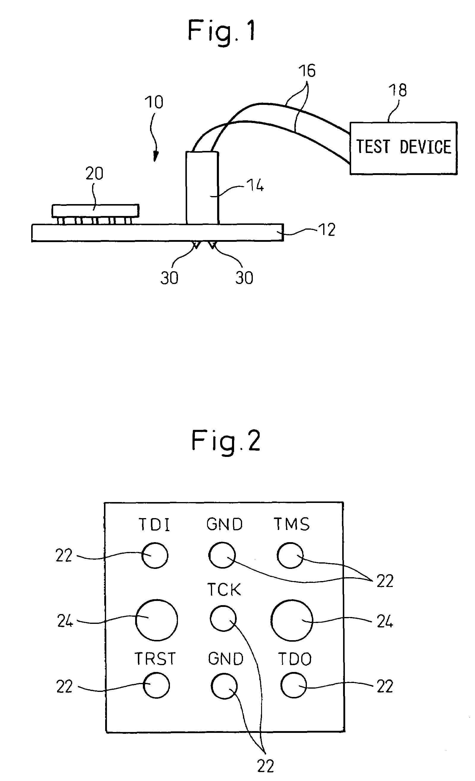
[0030]An embodiment of the present invention will be described with reference to the drawings below. FIG. 1 shows an example in which a connector according to the embodiment of the present invention is connected to a printed circuit board and a test device. FIG. 2 shows a region or part of the printed circuit board shown in FIG. 1 in which a plurality of electrode pads and a plurality of fixing holes are arranged. The region shown in FIG. 2 is equivalent to a region on the printed circuit board to which the connector shown in FIG. 1 is attached. A description will be made, by way of an example of an electrical connection, of an object to be tested, to a test device for in-circuit emulation, of a printed circuit board. However, the present invention is not limited to such an example.

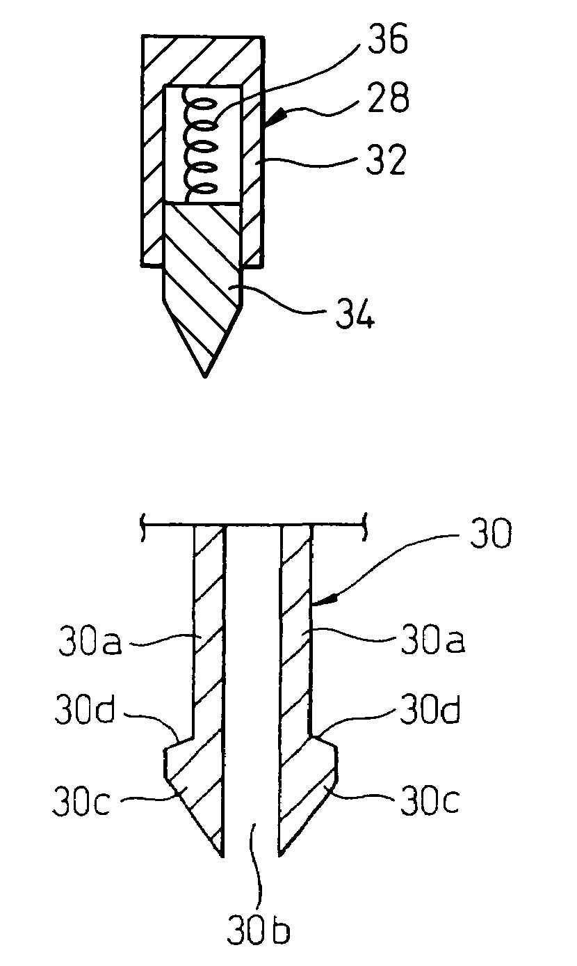
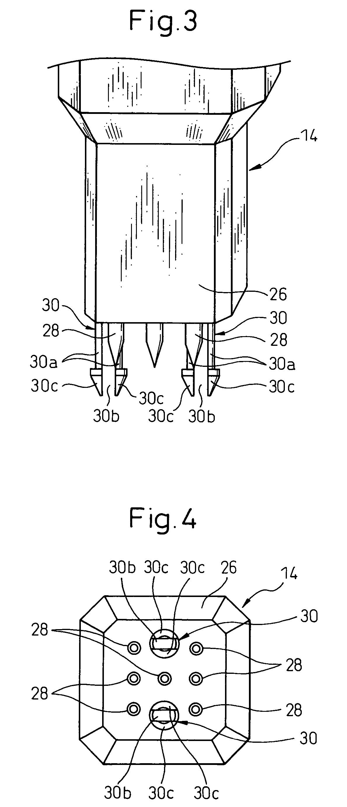
[0031]In FIGS. 1 and 2, an attached / assembled structure 10 comprises a printed circuit board 12 and a connector 14. The connector 14 is constructed to be attached to the printed circuit board 12, and to b...


PUM


Abstract

A connector has conducting pins projecting from a connector body, and fixing pin extending substantially in parallel with the conducting pins. The fixing pins are longer than the conducting pins. The fixing pins are constructed such that they can be inserted in corresponding fixing holes of a printed circuit board when the connector is attached to the printed circuit board. The fixing pins are locked in the fixing holes to secure the electrical connection between the conducting pins and corresponding electrode pads and the mechanical connection between the connector and the printed circuit board.

Description

BACKGROUND OF THE INVENTION[0001]1. Field of the Invention[0002]The present invention relates to a connector.[0003]2. Description of the Related Art[0004]In a test of a printed circuit board, a plurality of probes connected to a test device are arranged, in the same pattern as the pattern of electrode pads on the printed circuit board, and are brought into contact with the respective electrode pads. Spring probes are used as the testing probes. The spring probes are arranged in a jig, so that the spring probes are pressed against the electrode pads on the printed circuit board. This method makes it necessary to develop and manufacture jigs in line with printed circuit boards, and the cost of development and manufacture of a jig arises for each type of printed circuit board. Moreover, the jig bearing the spring probes has a relatively complex structure and a mechanism for supporting the printed circuit board is needed.[0005]As a method of connecting a printed circuit board to a test ...

Claims


Application Information

Patent Timeline
Patent Type & Authority Patents(United States)
IPC IPC(8): H01R13/73G01R31/02G01R1/06H01R12/00H01R12/53H01R12/71H01R12/75H01R12/77H01R13/24H01R13/639
CPCG01R1/0416H05K1/0268H01R12/7023G01R31/2815H05K1/0219H05K3/301H05K2201/09063H05K2201/10598
Inventor BABA, MASAYUKIKAMEYAMA, SHUICHI
Owner FUJITSU LTD
Why Eureka
Try Eureka