Reference voltage generating circuit for integrated circuit

a voltage generation circuit and reference voltage technology, applied in the direction of electric variable regulation, process and machine control, instruments, etc., can solve the problems of unstable or even disabled, unstable current mirror operation of the second current mirror section, and consume self-refresh power of the dram, so as to ensure the stability of operation

Inactive Publication Date: 2006-11-14
SAMSUNG ELECTRONICS CO LTD
View PDF5 Cites 14 Cited by
  • Summary
  • Abstract
  • Description
  • Claims
  • Application Information

AI Technical Summary

Benefits of technology

[0026]It is yet another feature of the present invention to provide a reference voltage generating circuit for an integrated circuit capable of stabilizing an initial current mirror operation when a driving power supply voltage is switched.
[0027]It is yet another feature of the present invention to provide a reference voltage generating circuit for an integrated circuit in which the circuit has a high-speed response characteristic and guarantees stability of operation.
[0040]According to the reference voltage generating circuit for an integrated circuit of the present invention, an initial current mirror operation can be stabilized in a short time when a driving power supply voltage is switched, thereby enhancing a high-speed response characteristic and stability of operation.

Problems solved by technology

The DRAM consumes self-refresh power due to the required self-refreshing operation.
First, if a high switching control signal EN is applied, the P-type MOS transistor PD1 is turned ON and in turn the P-type MOS transistors MP1 and MP2 of the first current mirror section begin to be turned ON. At this time, since the voltage level of the reference voltage output node a1 rises earlier than the voltage level of the node a2 because of properties of the circuit, the P-type MOS transistors MP1 and MP2 may be turned OFF before the voltage level at the node a2 rises to a sufficient level. In this case, since the voltage of the node a2 does not reach a required sufficient level, it causes the current mirror operation of the second current mirror section, which is composed of the N-type MOS transistors MN1 and MN2, to be unstable or even to be disabled.
As such, an early turn-off operation of the P-type MOS transistors MP1 and MP2 in a period for which the driving power supply voltage VDD is initially supplied makes the current mirror operation of the second current mirror section unstable.
Accordingly, a time period until the voltage level of the reference voltage output node a1 is set to a normal voltage level is long, resulting in deterioration of high-speed response characteristics of the circuit.
Therefore, the circuit has a problem in that a high-speed response characteristic is degraded.
Further, there is a problem in that if particular nodes become in a floating state upon power-off, more time is initially taken until the voltage level is stabilized upon next power application.

Method used


Image

  • Reference voltage generating circuit for integrated circuit
  • Reference voltage generating circuit for integrated circuit
  • Reference voltage generating circuit for integrated circuit

Examples


Embodiment Construction

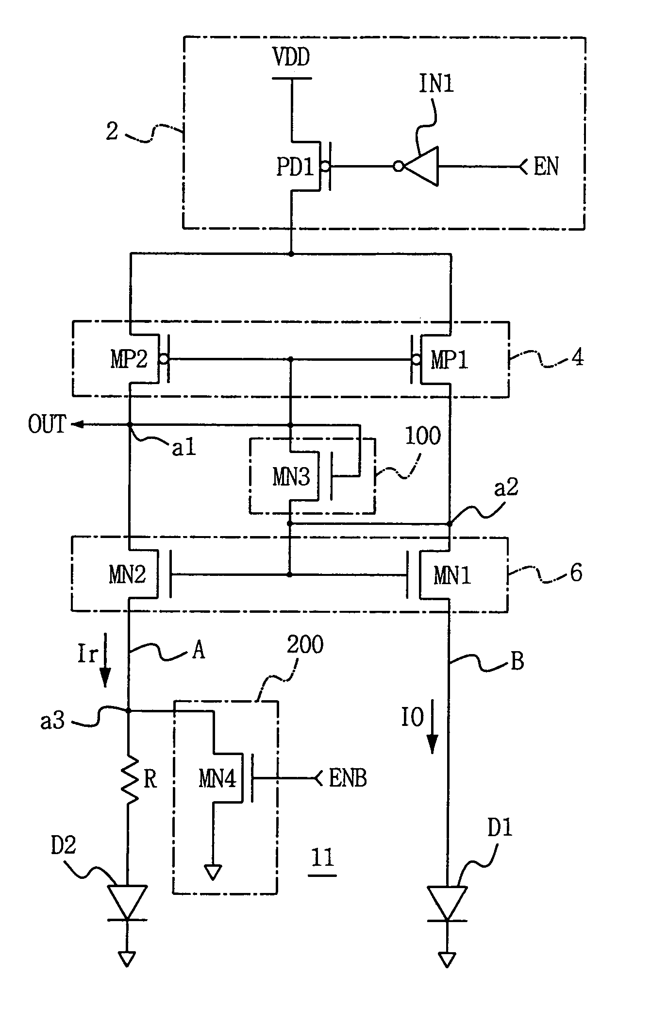
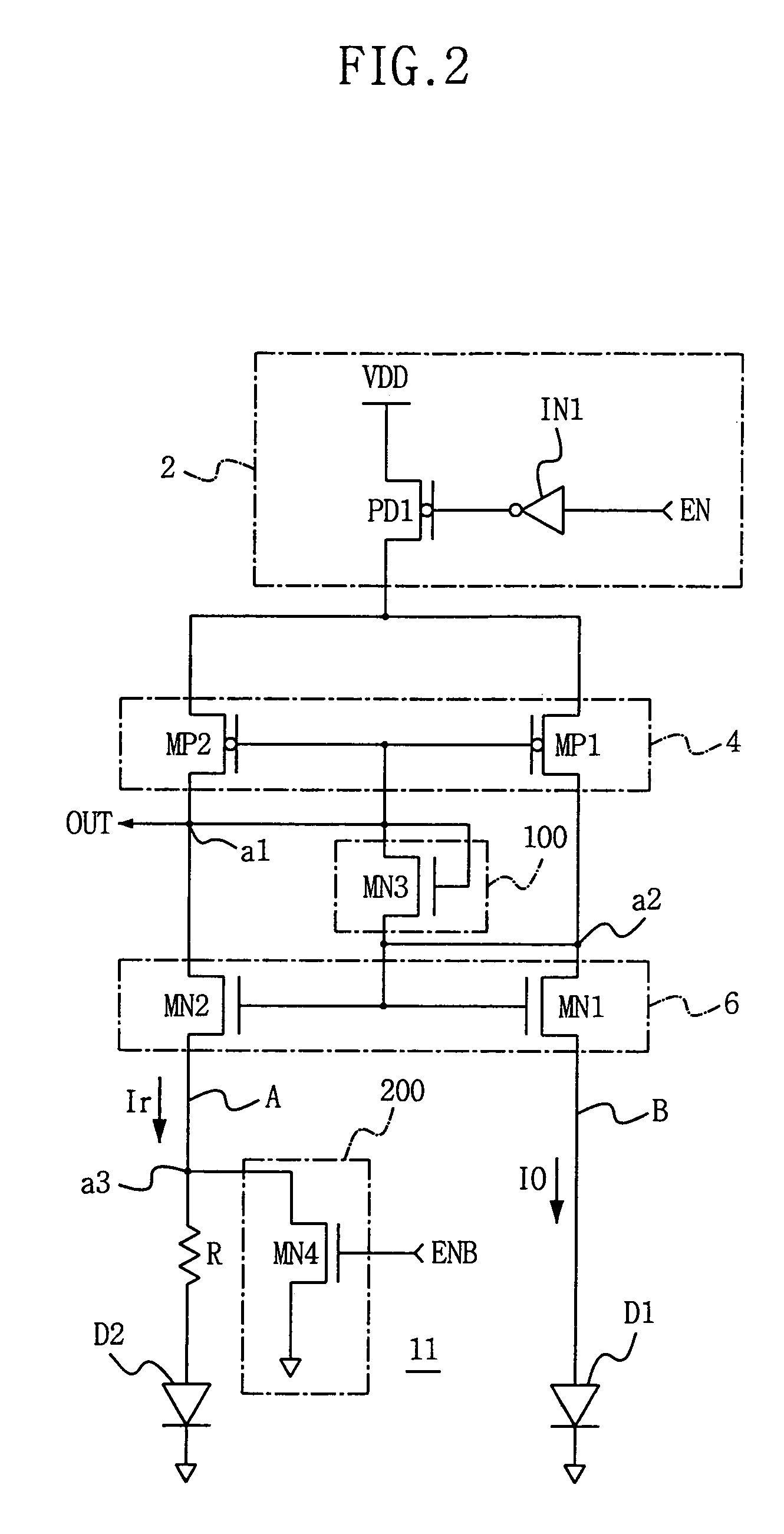
[0047]FIG. 2 is a diagram showing a reference voltage generating circuit according to an embodiment of the present invention. Referring to the figure, shown is a reference voltage generating circuit 11 comprising a charge transporting section 100 connected between a gate terminal of a first MOS transistor MP2 of a first conductivity type in a first current mirror 4 and a gate terminal of a fourth MOS transistor MN1 of a second conductivity type in a second current mirror 6, and a current sink section 200 for connecting a source terminal of a third MOS transistor MN2 of the second conductivity type to a ground voltage VSS in response to a second switching control signal ENB, in addtion to the configuration of FIG. 1 including a driving switching section 2. Although not shown, a filter section may be employed, which is connected in parallel with diodes D2 and Dl and to a ground to eliminate switching noise.

[0048]The charge transporting section 100 may include a fifth MOS transistor MN...


PUM


Abstract

A reference voltage generating circuit has a power supply voltage node to which a driving power supply voltage is intermittently applied. The circuit includes; a first current mirror section including a first MOS transistor of a first conductivity type having a source terminal connected to the power supply voltage node and a gate terminal connected to a drain terminal as a reference voltage output node, and a second MOS transistor of the first conductivity type having a gate terminal connected to the gate terminal of the first MOS transistor of the first conductivity type and a source terminal connected to the power supply voltage node; a second current mirror section including a third MOS transistor of a second conductivity type having a drain terminal connected to the reference voltage output node and a source terminal connected to a first current path to which a first resistor and a first diode are serially connected, and a fourth MOS transistor of the second conductivity type having a gate terminal and a drain terminal connected to the gate terminal of the third MOS transistor of the second conductivity type in common and a source terminal connected to the second current path to which a second diode is serially connected; and a charge transporting section connected between the gate terminal of the first MOS transistor of the first conductivity type in the first current mirror section and the gate terminal of the fourth MOS transistor of the second conductivity type in the second current mirror section.

Description

CROSS-REFERENCE TO RELATED APPLICATION[0001]This application claims the benefit of Korean Patent Application No. 2003-0075749, filed on Oct. 29, 2003, the contents of which are hereby incorporated herein by reference in their entirety.BACKGROUND[0002]1. Technical Field[0003]The present invention relates to a reference voltage generating circuit for an integrated circuit and, more particularly, to a reference voltage generating circuit for an integrated circuit for use in an on-chip temperature sensor.[0004]2. Discussion of the Related Art[0005]Generally, a variety of semiconductor devices implemented by integrated circuit chips such as CPUs, memories, gate arrays or the like are used in a variety of electrical products, such as portable personal computers, personal digital assistants (PDAs), servers, portable telephones, or workstations. Many of such electrical products implement a sleep mode to save power, in which most of the circuit components in the products remain in a turn-off...

Claims


Application Information

Patent Timeline
Patent Type & Authority Patents(United States)
IPC IPC(8): G05F3/24G05F3/26G05F3/02G11C5/14G05F3/30
CPCG05F3/30G11C5/14
Inventor MIN, YOUNG-SUNKIM, NAM-JONG
Owner SAMSUNG ELECTRONICS CO LTD
Why Eureka
Try Eureka