Transimpedance amplifier

a technology of transimpedance amplifier and amplifier, applied in the field of electrical equipment, can solve problems such as wide bandwidth, and achieve the effects of wide bandwidth, large output voltage, and reduced equivalent input noise curren

Inactive Publication Date: 2006-11-14
SIRES LABS
View PDF6 Cites 48 Cited by
  • Summary
  • Abstract
  • Description
  • Claims
  • Application Information

AI Technical Summary

Benefits of technology

[0018]The present invention provides a transimpedance amplifier, which is useful as an optical fiber preamplifier. The illustrative embodiment is advantageous in four ways. First, it minimizes the equivalent input noise current. Second, it has a wide bandwidth. Third, it has a reasonably large output voltage, and fourth, it is stable over wide temperature and voltage ranges.
[0019]The illustrative embodiment comprises a transimpedance stage and a gain stage. The transimpedance stage has a low input impedance to minimize input noise current. Both stages employ a pure NMOS design which contributes stability over temperature and power supply fluctuations. Gain is increased by the gain stage. Bandwidth is increased over the prior art by replacing R1 in FIG. 2 by an inductive load. A monolithic inductor on an integrated circuit is quite large, so instead of using a monolithic inductor, the illustrative embodiment employs an “active” inductor: the combination of a resistor connected in series with the gate of an NMOS transistor, where the potential at the drain of the NMOS transistor is held below that of the second terminal of the resistor by at least the threshold, or turn-on voltage, of the transistor. This transistor / resistor combination acts inductively at the data rates of interest. These active inductors are also employed in the gain stage of the illustrative embodiment to improve bandwidth.

Problems solved by technology

Second, it has a wide bandwidth.

Method used


Image

  • Transimpedance amplifier
  • Transimpedance amplifier
  • Transimpedance amplifier

Examples


Embodiment Construction

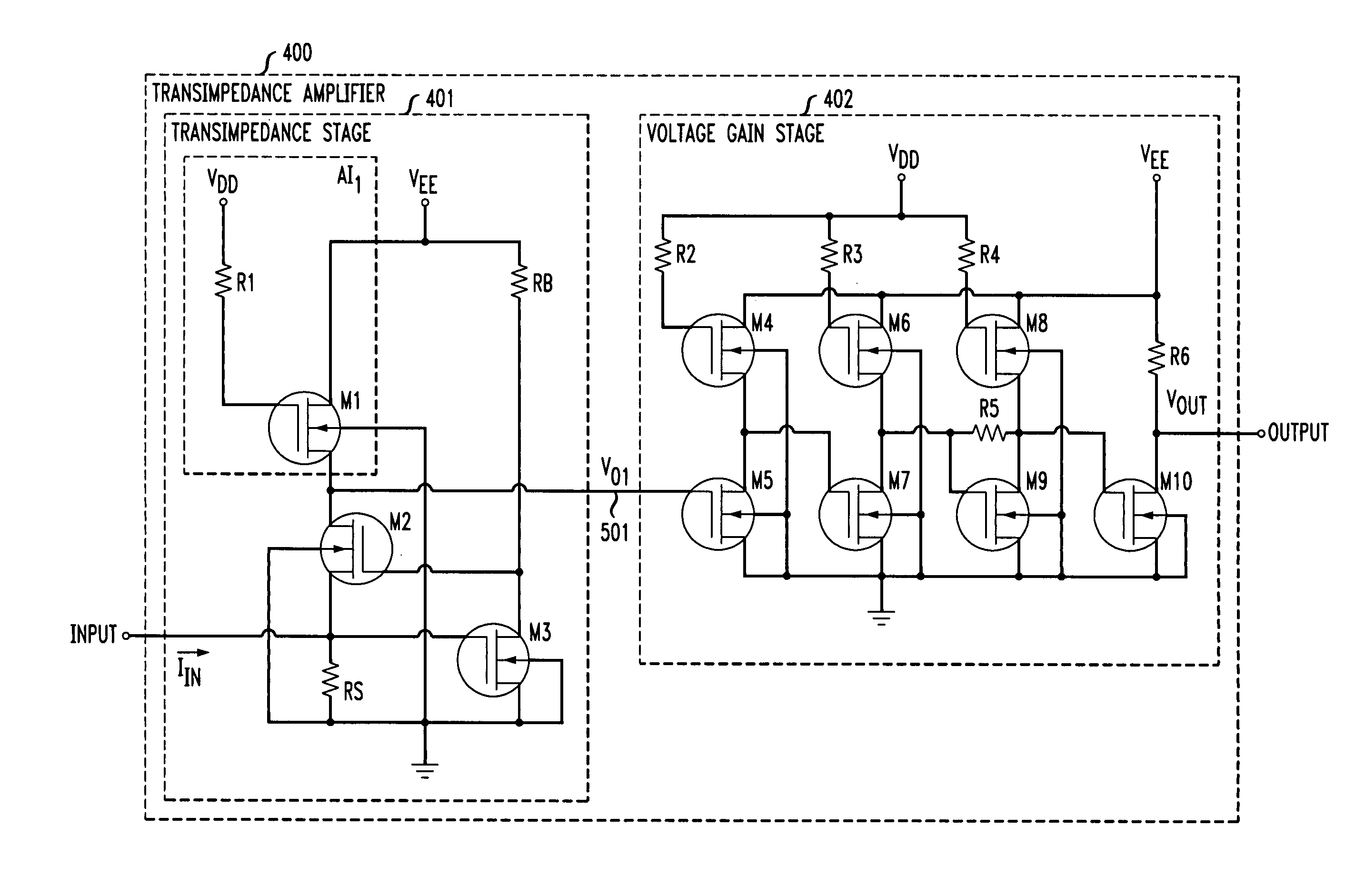
[0031]FIG. 6 depicts a block diagram of a transimpedance amplifier in accordance with the illustrative embodiment of the present invention. The transimpedance amplifier 400 comprises transimpedance stage 401 and voltage gain stage 402.

[0032]FIG. 7 depicts a schematic diagram of a transimpedance amplifier in accordance with the illustrative embodiment of the present invention. The illustrative embodiment comprises: eight resistors, R1 through R6, RS, and RB, and ten transistors, M1 through M10. In accordance with the illustrative embodiment, transistors M1 through M10 are N-Type Enhancement mode transistors, as are well-known to those skilled in the art.

[0033]Transimpedance stage 401 has a terminal labeled INPUT into which the input current is injected. This INPUT terminal is electrically connected to the gate of transistor M3, the source of transistor M2, and one terminal of resistor RS. The second terminal of RS and the source terminal of transistor M3 are connected to ground poten...


PUM


Abstract

A transimpedance amplifier, which is useful as an optical fiber preamplifier, is disclosed. The illustrative embodiment exhibits four characteristics. First, it minimizes the equivalent input noise current. Second, it has a wide bandwidth. Third, it has a reasonably large output voltage, and fourth, it is stable over wide temperature and voltage ranges. The illustrative embodiment comprises a transimpedance stage and a gain stage. Both stages employ a pure NMOS design which contributes to the above four advantages. Bandwidth is further increased over the prior art by the use of inductive loads. The inductive loads of the illustrative embodiment are not physical inductors, but transistor-based “active” inductors: the combination of a resistor connected in series with the gate of an NMOS transistor.

Description

FIELD OF THE INVENTION[0001]The present invention relates to electronics in general, and, more particularly, to a transimpedance amplifier design.BACKGROUND OF THE INVENTION[0002]Modern optical telecommunications systems often employ optical fibers for carrying signals. Low-cost, high-performance, highly integrated fiber optic interface circuits are becoming increasingly necessary to meet the demands of high-speed digital data communication. One standard circuit function for fiber optic communication systems is a transimpedance amplifier that is used within an optical receiver.[0003]FIG. 1 depicts an architectural diagram of a typical optical receiver. The light from an optical fiber 101 impinges on photodiode detector 102, producing a current IPD. Transimpedance amplifier 103 converts the very small currents indicative of optical signals applied to photodetector 102 into a large signal voltage, VTIA, which is further amplified by post amplifier 104 to voltage VPA for output to digi...

Claims


Application Information

Patent Timeline
Patent Type & Authority Patents(United States)
IPC IPC(8): H03F3/08
CPCH03F3/082
Inventor QUADIR, NASIR ABDULALIAS, FARRAH AZLIN BINTIKRISHNARAJOO, K. SELVARAJAH K.
Owner SIRES LABS
Why Eureka
Try Eureka