Method, system and circuit for programming a non-volatile memory array

a non-volatile memory and array technology, applied in the field of non-volatile memory (“ nvm”) cells, can solve the problems of increasing the programming tail, reducing the nvm's threshold voltage, and increasing the charge in the cell, so as to achieve the effect of lowering the programming rate and reducing the programming variation

Inactive Publication Date: 2006-11-14
SAIFUN SEMICONUCTIORS
View PDF133 Cites 65 Cited by
  • Summary
  • Abstract
  • Description
  • Claims
  • Application Information

AI Technical Summary

Benefits of technology

[0015]The present invention is a method circuit and system for programming non-volatile memory (“NVM”) cells in an NVM array. According to some embodiments of the present invention, one or more NVM cells of a memory array may be programmed using a controller or programming circuit adapted to provide a first programming phase and a second programming phase, wherein programming pulses associated with the second programming phase may induce lower programming rate, hence lower programming variations.

Problems solved by technology

While the amount of charge in the cell may decrease by applying an erase pulse to the NVM cell which may force the charge reduction in the cell's charge storage region, and consequently may decrease the NVM's threshold voltage.
This is reflected in the programming tail that may become larger using more aggressive algorithms.
Larger Programming tails may not be wanted since they reduce the endurance and retention figures of an NVM cell.
The simple solution of reducing the steps of a programming algorithm to smaller and smaller steps does not assure the similar reduction of the PGM tail voltage distribution.
This is due to practical limitations of array non uniformities in many parameters (e.g. physical dimensions, resistances of current paths, number of cells that need programming pulses simultaneously, etc. . . . ).

Method used


Image

  • Method, system and circuit for programming a non-volatile memory array
  • Method, system and circuit for programming a non-volatile memory array
  • Method, system and circuit for programming a non-volatile memory array

Examples


Embodiment Construction

[0042]In the following detailed description, numerous specific details are set forth in order to provide a thorough understanding of the invention. However it will be understood by those of ordinary skill in the art that the present invention may be practiced without these specific details. In other instances, well-known methods and procedures have not been described in detail so as not to obscure the present invention.

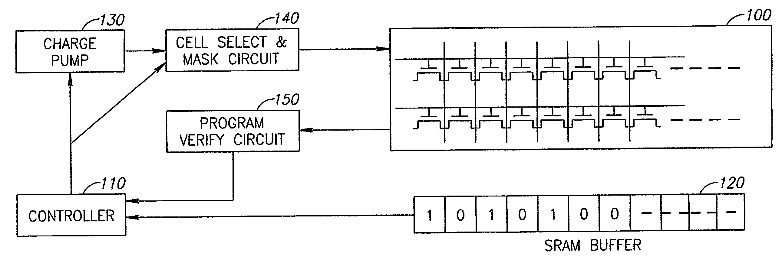
[0043]The present invention is a method circuit and system for programming non-volatile memory (“NVM”) cells in an NVM array. According to some embodiments of the present invention, one or more NVM cells of a memory array may be programmed using a controller or programming circuit adapted to provide a first programming phase and a second programming phase, wherein programming pulses associated with the second programming phase may induce relatively greater threshold voltage changes in cells having less stored charge than in cells having relatively more stored charge.

[...


PUM


Abstract

The present invention is a multi-phase method, circuit and system for programming non-volatile memory (“NVM”) cells in an NVM array. The present invention may include a controller to determine when, during a first programming phase, one or more NVM cells of a first set of cells reaches or exceeds to first intermediate voltage, and to cause a charge pump circuit to apply to a terminal of the one or more cells in the first set second phase programming pulses to induce relatively greater threshold voltage changes in cells having less stored charge than in cells having relatively more stored charge.

Description

CROSS-REFERENCE TO RELATED APPLICATIONS[0001]The present application claims priority from U.S. provisional patent application Ser. No. 60 / 421,786, filed Oct. 29, 2002, which is hereby incorporated by reference in its entirety.FIELD OF THE INVENTION[0002]The present invention generally relates to the field of non-volatile memory (“NVM”) cells. More specifically, the present invention relates to a system, circuit and method for programming one or more NVM cells using a multi-phase programming sequence or algorithm.BACKGROUND OF THE INVENTION[0003]Non-volatile memory (“NVM”) cells are fabricated in a large variety of structures, including but not limited to Poly-silicon floating gate, as shown in FIG. 2A, and Nitride Read Only Memory (“NROM”), as shown in FIG. 2B. As is well known, an NVM cell's state may be defined and determined by its threshold voltage, the gate to source voltage at which the cell begins to significantly conduct current.[0004]Different threshold voltage ranges are a...

Claims


Application Information

Patent Timeline
Patent Type & Authority Patents(United States)
IPC IPC(8): G11C11/34G11C11/56G11C16/04G11C16/10G11C16/34
CPCG11C11/5628G11C16/3468G11C16/10G11C11/5671
Inventor COHEN, GUYEITAN, BOAZ
Owner SAIFUN SEMICONUCTIORS
Why Eureka
Try Eureka