Multilayer waveguide filter employing via metals

Inactive Publication Date: 2006-11-28
ELECTRONICS & TELECOMM RES INST
View PDF11 Cites 36 Cited by
  • Summary
  • Abstract
  • Description
  • Claims
  • Application Information

AI Technical Summary

Problems solved by technology

A filter is the most complicated component among various electric components in a typical wireless communication system for miniaturizing and downing a cost.
Accordingly, a conventional waveguide filter occupies a large area in a wireless communication system and a manufacturing cost of the conventional waveguide filter is high.
How

Method used


Image

  • Multilayer waveguide filter employing via metals
  • Multilayer waveguide filter employing via metals
  • Multilayer waveguide filter employing via metals

Examples


Embodiment Construction

[0019]Hereinafter, a waveguide filter formed with a plurality of via metals in accordance with a preferred embodiment of the present invention will be described in more detail with reference to the accompanying drawings.

[0020]There are provided in FIGS. 1 to 5 illustrating various views of a waveguide filter provided with a plurality of via metals. It should be noted that like parts appearing in FIGS. 1 to 5 are represented by like reference numbers.

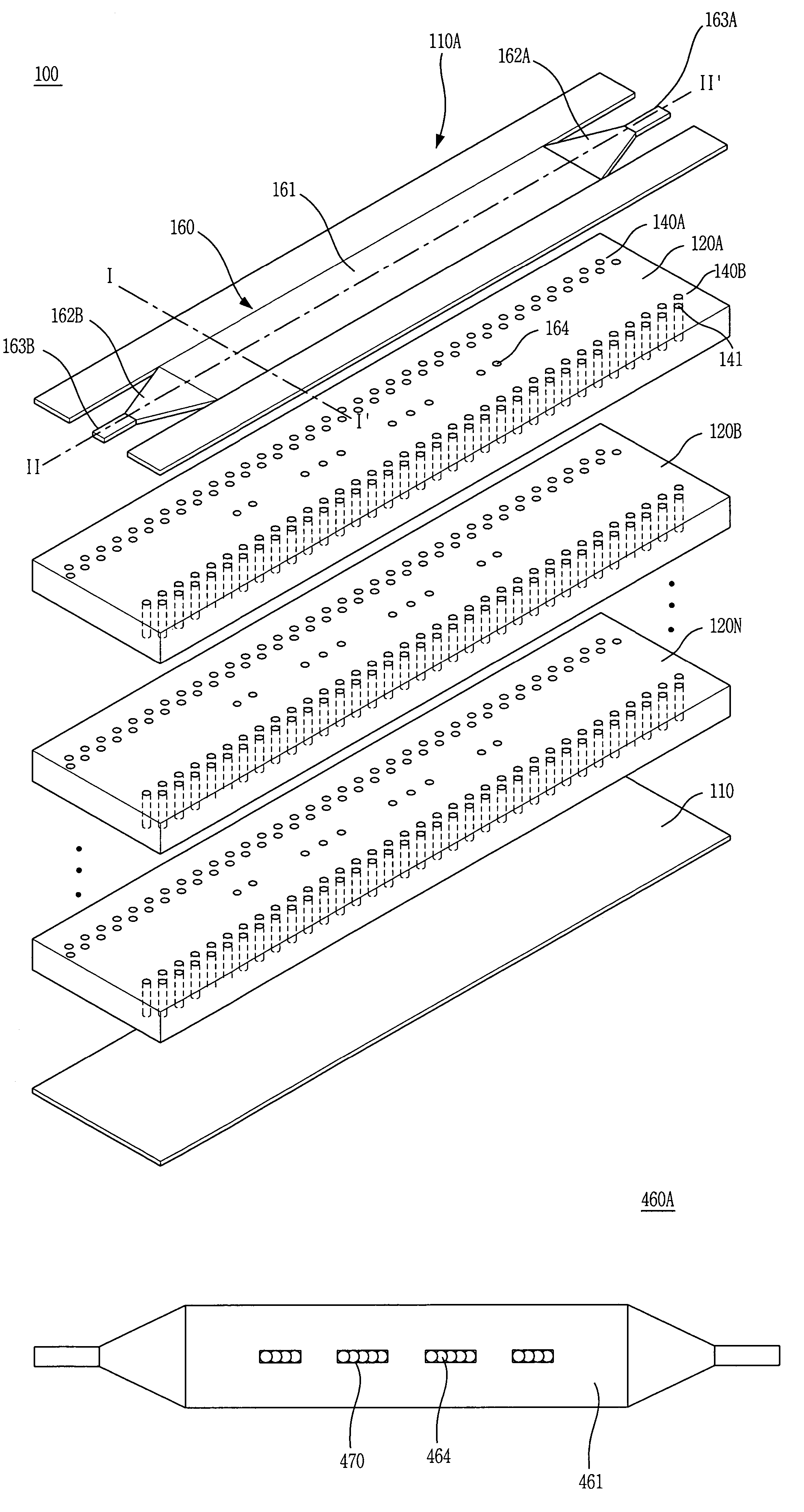
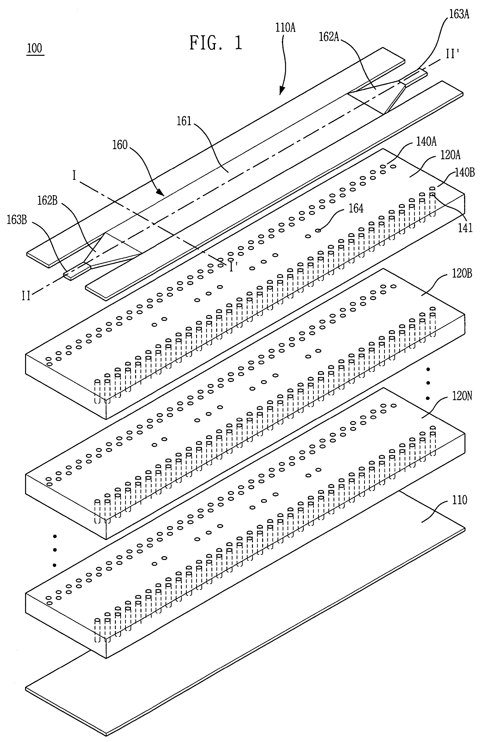
[0021]FIG. 1 is an exploded view illustrating a waveguide filter in accordance with a preferred embodiment of the present invention.

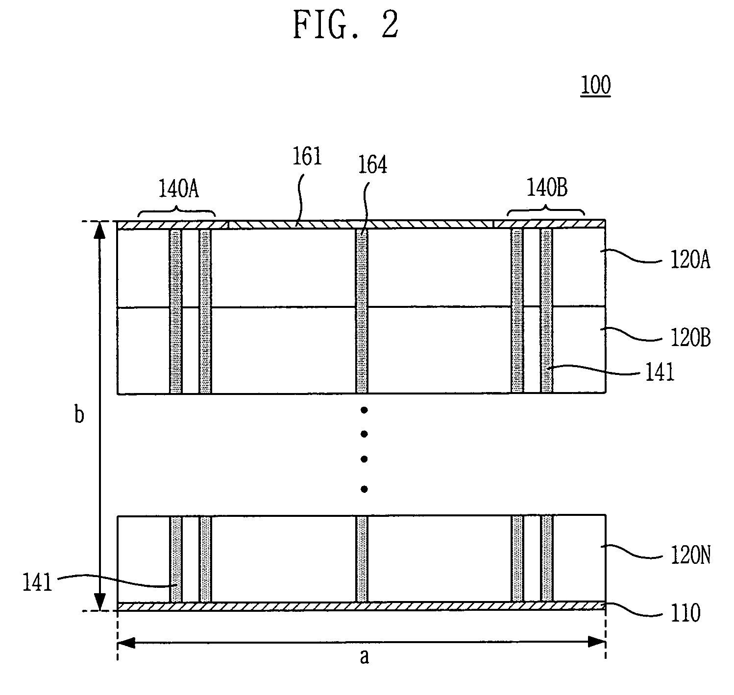
[0022]As shown, the waveguide filter 100 includes a lower conductive layer 110, N number of dielectric layers 120A, 120B, . . . 120N, stacked on the lower conductive layer 110 and an upper conductive layer 110A formed on the first dielectric layers 120A, wherein the lower and the upper conductive layers 110A, 110B serve as a ground. A first and a second side wall via patterns 140A, 140B are formed in both si...


PUM


Abstract

A waveguide filter is disclosed. The waveguide filter includes a lower conductive layer; a plurality of dielectric layers stacked on the lower conductive layer; an upper conductive layer formed on a top surface of the plurality of dielectric layers; a waveguide formed on the upper conductive layer; and two sets of first via metals arranged at longitudinal sides of the waveguide filter, wherein each of the sets is formed in two-fold line shape.

Description

FIELD OF THE INVENTION[0001]The present invention relates to a waveguide filter; and, more particularly, to a waveguide filter employing a multilayer ceramic structure for passing a selected frequency by using a plurality of via metals.DESCRIPTION OF RELATED ARTS[0002]Recently, a wireless communication technology has been developed to an international mobile telecommunication-2000 (IMT-2000), which is a 3rd generation wireless communication system and now, we expect that the communication system will be developed to a 4th generation of wireless communication technology in the near future.[0003]In the 4th generation of wireless communication technology, it is expected that mass amount of video and audio data are transmitted in a speed of 100 Mbps by using a millimeter wave.[0004]Generally, a miniaturization and a cost-effectiveness are major factors in developing a wireless communication system for processing a millimeter wave. A filter is the most complicated component among various...

Claims


Application Information

Patent Timeline
IPC IPC(8): H01P1/208H01P1/203H01P1/207H01P3/12
CPCH01P1/207H01P3/122H01P1/203H01P1/208
Inventor KIM, BONG-SUSONG, MYUNG-SUN
Owner ELECTRONICS & TELECOMM RES INST
Why Eureka
Try Eureka