
Polishing method

a technology of polishing method and polishing plate, which is applied in the direction of lapping machines, manufacturing tools, semiconductor devices, etc., can solve the problems of short circuit, large step height on the surface of the semiconductor device, and complicated structure of the semiconductor element, so as to prevent the effect of being dropped off and damaged

Inactive Publication Date: 2007-01-16
EBARA CORP
View PDF12 Cites 10 Cited by
  • Summary
  • Abstract
  • Description
  • Claims
  • Application Information

AI Technical Summary

Benefits of technology

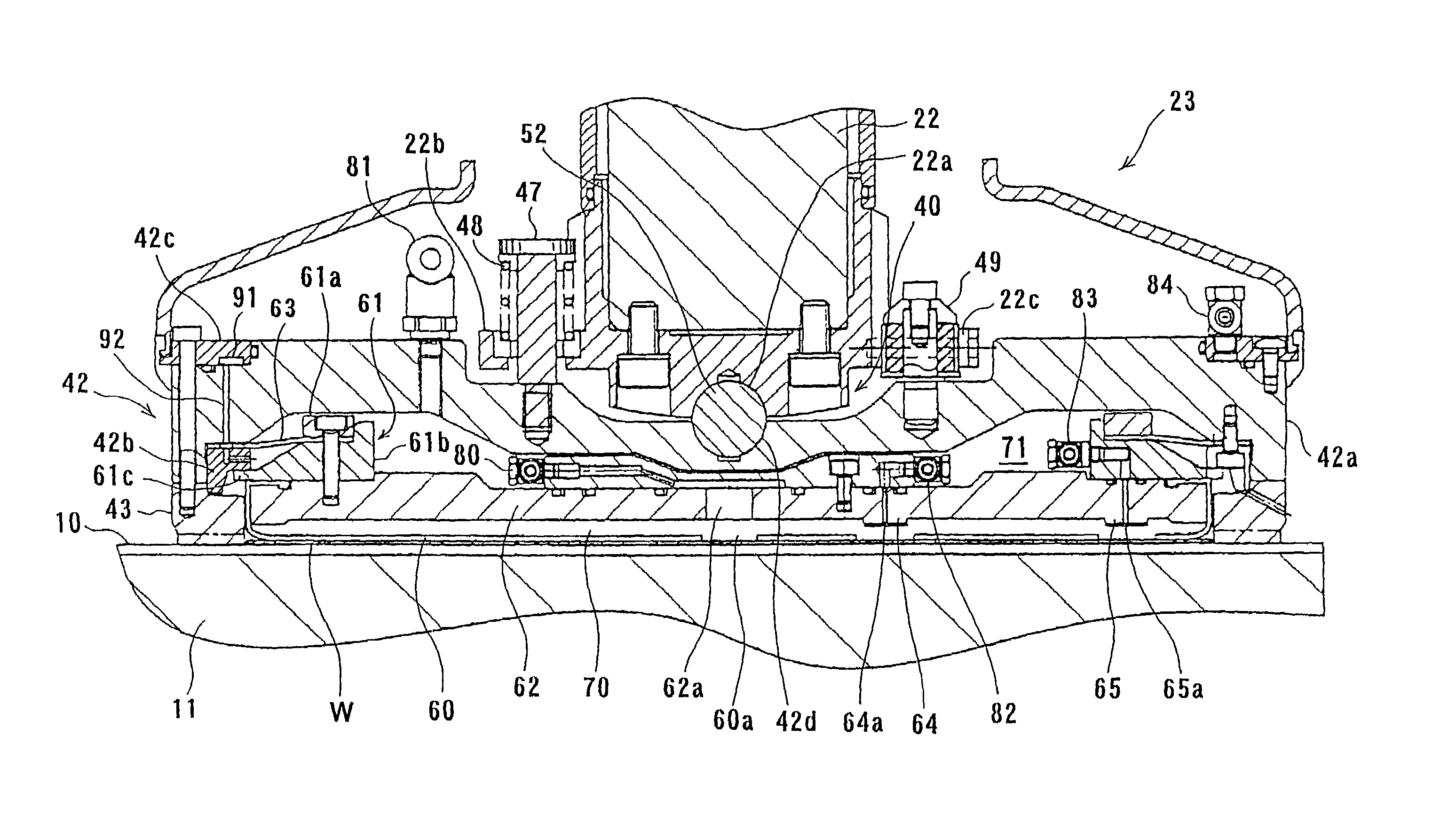
[0010]The present invention has been made in view of the above drawbacks. It is an object of the present invention to provide a polishing method which can reliably attract and release a workpiece, to be polished, even if the workpiece is held and polished using an elastic membrane.
[0012]When the pressurized fluid is ejected from the opening defined centrally in the vertically movable member, the pressurized fluid is delivered into the region where the elastic membrane and the workpiece are held in close contact with each other. Therefore, the workpiece can reliably be released.
[0014]Since the pressurized fluid is ejected not only from the opening defined centrally in the vertically movable member, but also from the hole in the elastic membrane, the workpiece can be released more reliably.
[0016]According to the present invention, it is possible to break the close contact between the elastic membrane and the workpiece, for thereby releasing the workpiece more reliably.
[0018]When the polishing process is finished, the workpiece and the vertically movable member may have occasionally been spaced from each other. In such a case, the attraction section fails to attract the workpiece even if the attraction section attempts to attract the workpiece. According to the present invention, when the polishing process is finished, the vertically movable member is moved downwardly to bring the workpiece into close contact with the attraction section, and thereafter the attraction section attracts and holds the workpiece. Consequently, it is possible to reliably attract the workpiece.
[0020]If the vertically movable member projects downwardly from the retainer ring and the workpiece is attracted at a displaced position when the workpiece is transferred, then the workpiece tends to be caught by the retainer ring when the vertically movable member is moved upwardly in a subsequent motion, thus causing the workpiece to be dropped off and damaged. According to the present invention, since the vertically movable member is positioned upwardly with respect to the retainer ring in advance, the workpiece is transferred while the outer circumferential portion thereof is guided by the retainer ring. Therefore, the workpiece is not caught by the retainer ring when the vertically movable member is moved upwardly, and hence the workpiece can be prevented from being dropped off and damaged.

Problems solved by technology

In recent years, semiconductor devices have become more integrated, and structures of semiconductor elements have become more complicated.
Accordingly, irregularities on a surface of a semiconductor device become increased, so that step heights on the surface of the semiconductor device tend to be larger.
When the number of irregularities is increased on the surface of the semiconductor device, the following problems arise.
An open circuit is caused by disconnection of interconnections, or a short circuit is caused by insufficient insulation between interconnection layers.
As a result, good products cannot be obtained, and the yield tends to be reduced.
Further, even if the semiconductor device initially works normally, the reliability of the semiconductor device is lowered after a long-term use.
Therefore, if the irregularities of the surface of the semiconductor device are increased, then it becomes problematic that it is difficult to form a fine pattern itself on the semiconductor device.
In such a polishing apparatus, if a relative pressing force between the semiconductor wafer being polished and the polishing surface of the polishing pad is not uniform over an entire surface of the semiconductor wafer, then the semiconductor wafer may insufficiently be polished or may excessively be polished at some portions depending on the pressing force applied to those portions of the semiconductor wafer.
Further, the polishing pad is so elastic that the pressing force applied to a circumferential edge portion of the semiconductor wafer being polished becomes non-uniform, and hence only the circumferential edge portion of the semiconductor wafer may excessively be polished, which is called “edge rounding”.
However, the top ring using the above elastic membrane tends to fail in attracting and releasing the semiconductor wafer because of the presence of the elastic membrane.

Method used


Image

  • Polishing method
  • Polishing method
  • Polishing method

Examples


Embodiment Construction

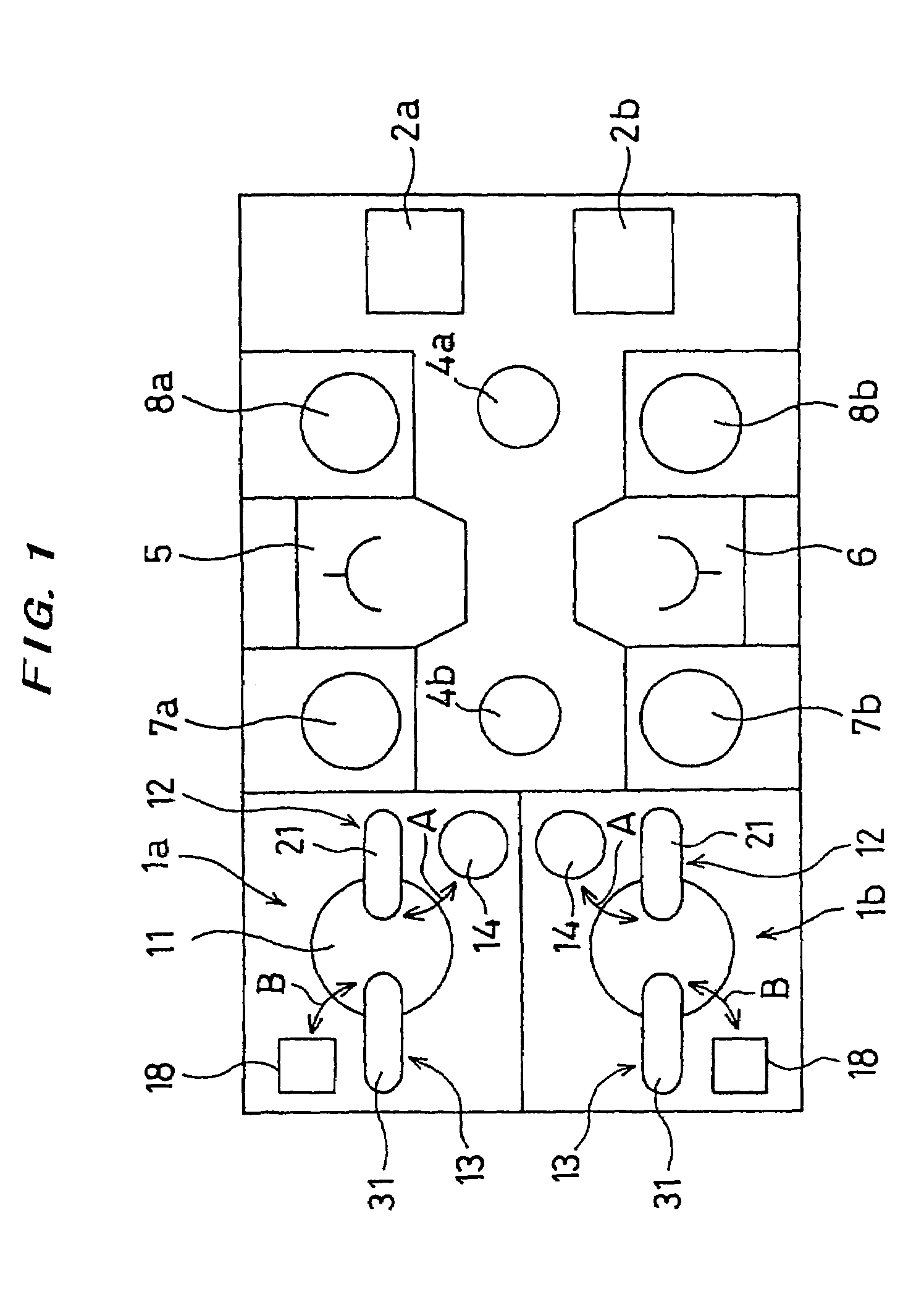
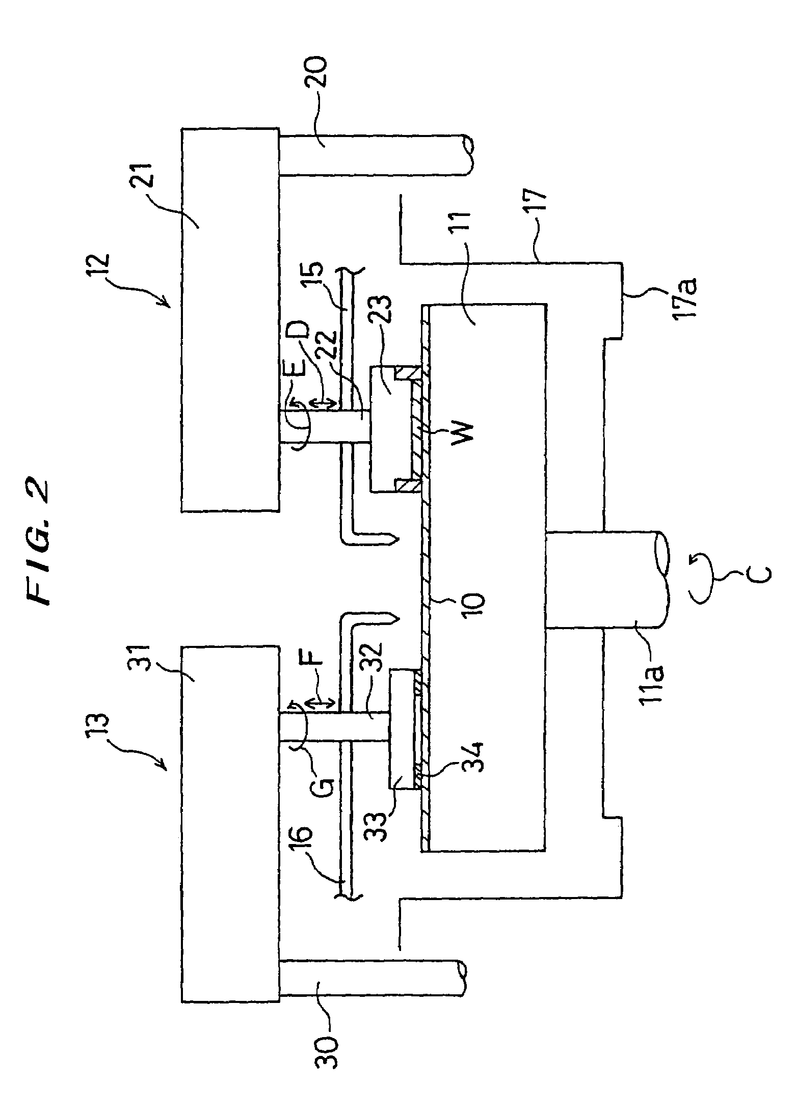
[0043]A polishing method according to a first embodiment of the present invention will be described below in detail with reference to FIGS. 1 through 12. FIG. 1 is a schematic plan view showing a polishing apparatus according to the first embodiment of the present invention. As shown in FIG. 1, in the polishing apparatus, a pair of polishing sections 1a, 1b are disposed at one side of a space on a floor having a rectangular shape so as to face each other. A pair of load / unload units for placing cassettes 2a, 2b thereon which accommodate semiconductor wafers are disposed at the other side. Two transfer robots 4a, 4b for transferring the semiconductor wafer are disposed on a line connecting the polishing sections 1a, 1b to the load / unload units, thus forming a transfer line. Reversing devices 5, 6 are disposed on each side of the transfer line, respectively, and cleaning devices 7a, 8a and cleaning devices 7b, 8b are disposed so as to interpose the respective reversing devices 5, 6 th...


PUM


Abstract

The present invention is relates to a polishing method for polishing a semiconductor wafer (W) by pressing the semiconductor wafer (W) against a polishing surface (10) with use of a top ring (23) for holding the semiconductor wafer (W). A pressure chamber (70) is defined in the top ring (23) by attaching an elastic membrane (60) to a lower surface of a vertically movable member (62). The semiconductor wafer (W) is polished while a pressurized fluid is supplied to the pressure chamber (70) so that the semiconductor wafer (W) is pressed against the polishing surface (10) by a fluid pressure of the fluid. The semiconductor wafer (W) which has been polished is released from the top ring (23) by ejecting the pressurized fluid from an opening (62a) defined centrally in the vertically movable member (62).

Description

[0001]This application is a PCT / JP03 / 04894 Apr. 17, 2003.TECHNICAL FIELD[0002]The present invention relates to a polishing method, and more particularly to a polishing method for polishing a workpiece, such as a semiconductor wafer having a thin film formed on a surface thereof, to a flat mirror finish.BACKGROUND ART[0003]In recent years, semiconductor devices have become more integrated, and structures of semiconductor elements have become more complicated. Further, the number of layers in multilayer interconnections used for a logical system has been increased. Accordingly, irregularities on a surface of a semiconductor device become increased, so that step heights on the surface of the semiconductor device tend to be larger. This is because, in a manufacturing process of the semiconductor device, a thin film is formed on the semiconductor device, then micro machining processes, such as patterning or forming holes, are performed on the semiconductor device, and these processes are...

Claims


Application Information

Patent Timeline
Patent Type & Authority Patents(United States)
IPC IPC(8): H01L21/302B24B37/005B24B37/30H01L21/304H01L21/306
CPCB24B37/013B24B37/042B24B37/30Y10S438/977H01L21/30625H01L21/304
Inventor TOGAWA, TETSUJIFUKUSHIMA, MAKOTOSAKURAI, KUNIHIKOYOSHIDA, HIROSHINABEYA, OSAMUICHIMURA, TERUHIKO
Owner EBARA CORP
Learn More