

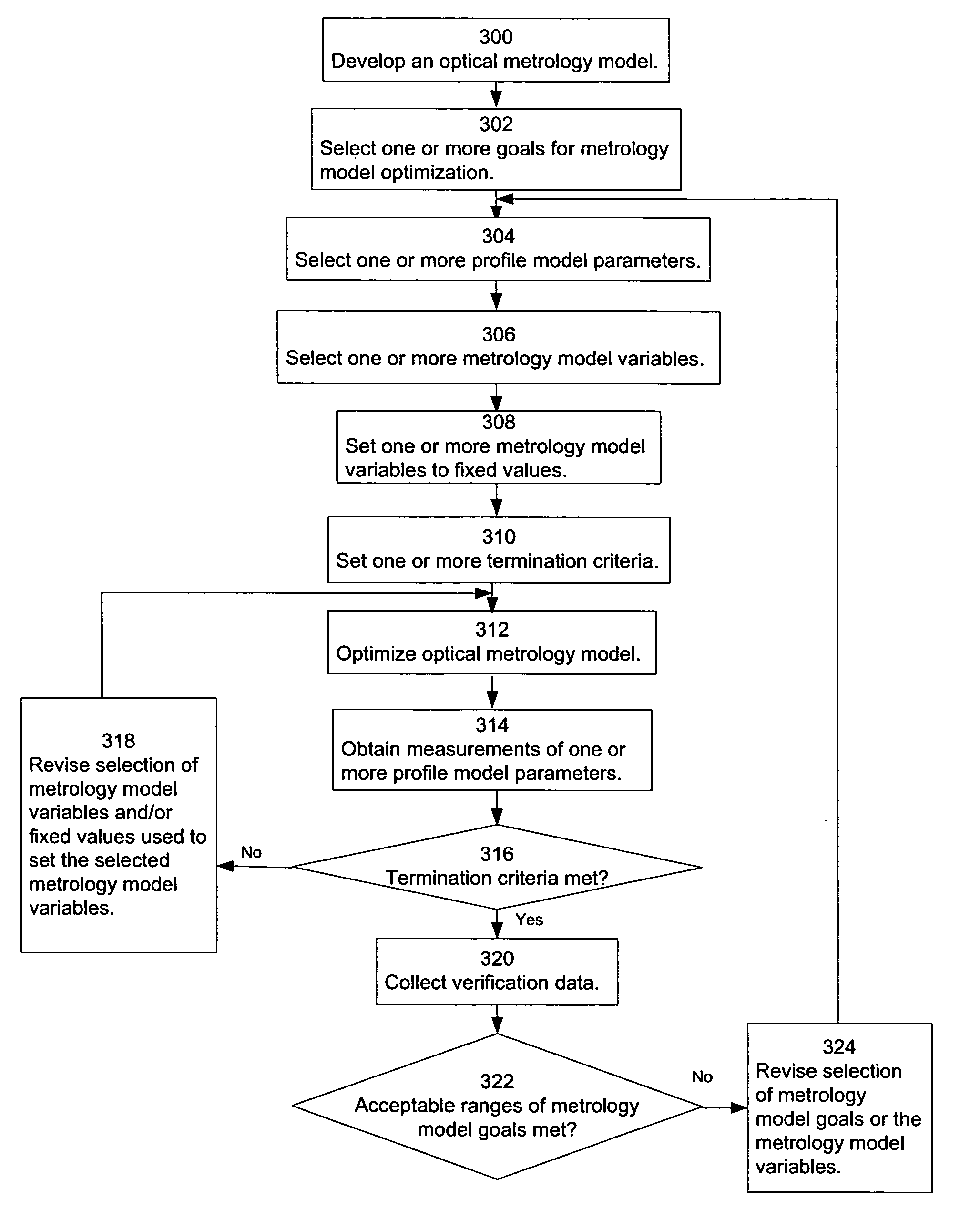
Optical metrology model optimization based on goals
a technology of optical metrology and optimization, applied in the field of optical metrology, can solve the problems of increasing the amount of time needed to develop the optical metrology model, allowing too many metrology model variables to produce erroneous measurements,
- Summary
- Abstract
- Description
- Claims
- Application Information
AI Technical Summary
Benefits of technology
Problems solved by technology
Method used
Image

Examples
Embodiment Construction
[0014]The following description sets forth numerous specific configurations, parameters, and the like. It should be recognized, however, that such description is not intended as a limitation on the scope of the present invention, but is instead provided as a description of exemplary embodiments.
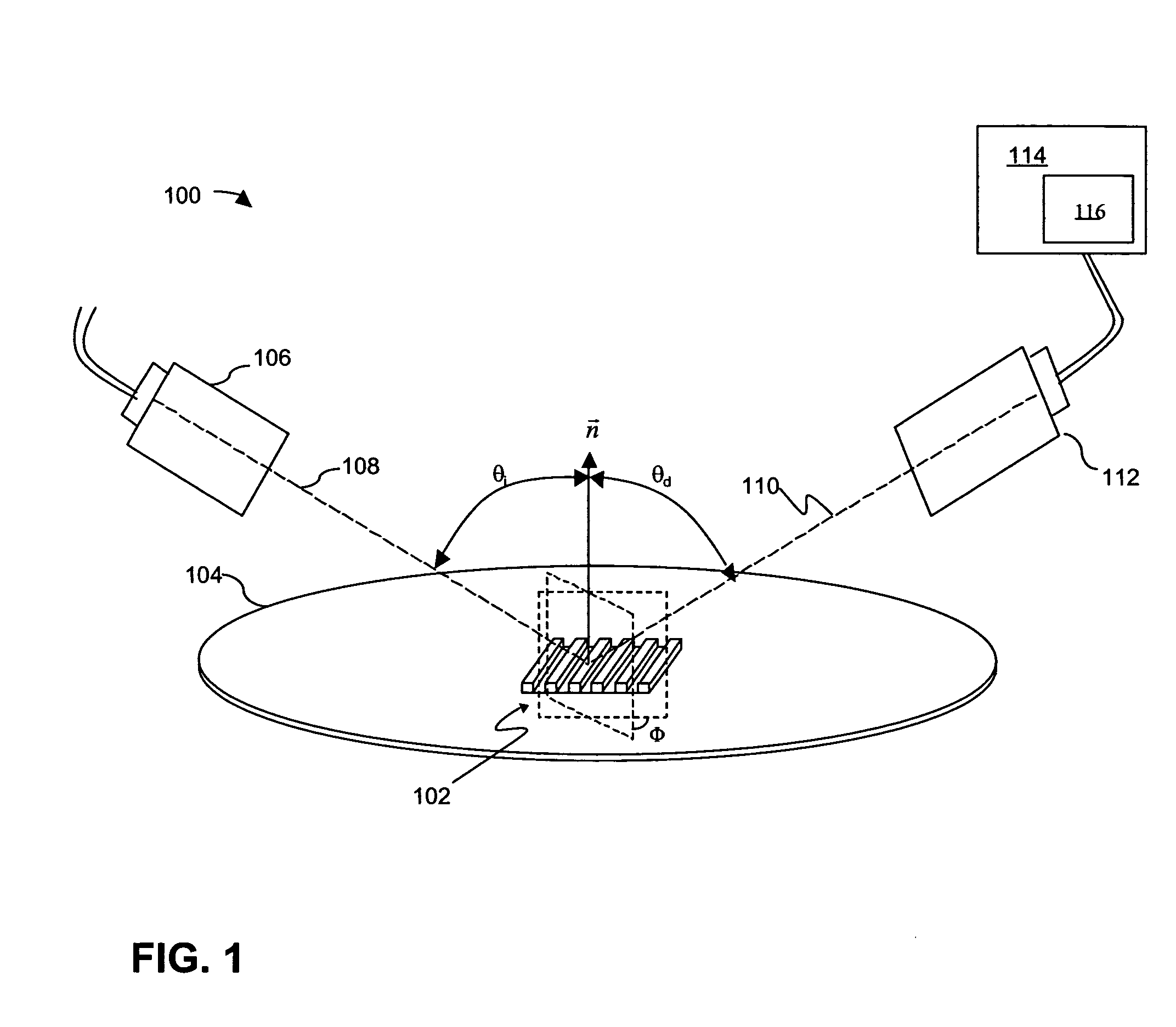
[0015]With reference to FIG. 1, an optical metrology system 100 can be used to examine and analyze a structure. For example, optical metrology system 100 can be used to determine the profile of a periodic grating 102 formed on wafer 104. As described earlier, periodic grating 102 can be formed in test areas on wafer 104, such as adjacent to a device formed on wafer 104. Alternatively, periodic grating 102 can be formed in an area of the device that does not interfere with the operation of the device or along scribe lines on wafer 104.
[0016]As depicted in FIG. 1, optical metrology system 100 can include a photometric device with a source 106 and a detector 112. Periodic gra...
PUM
 Abstract
Description
Claims
Application Information