ZnO/Cu(InGa)Se2 solar cells prepared by vapor phase Zn doping

a solar cell and cu(inga)se technology, applied in the direction of semiconductor/solid-state device manufacturing, electrical apparatus, semiconductor devices, etc., can solve the problems of slow wet chemical step, increase manufacturing costs, and complications remain

Inactive Publication Date: 2007-02-20
ALLIANCE FOR SUSTAINABLE ENERGY
View PDF13 Cites 155 Cited by
  • Summary
  • Abstract
  • Description
  • Claims
  • Application Information

AI Technical Summary

Benefits of technology

[0010]One object of the present invention is to provide an improved process for making CuInGaSe2 thin film solar cells characterized by conversion efficiencies greater than about 11%, and yet avoid the need to deposit a buffer layer.

Problems solved by technology

“While various improvements have been made in the manufacture of copper indium diselenide CdS cells, several complications remain.
However, this step involves a slow wet chemical step inconsistent with an otherwise in-line dry fabrication process.
Moreover, cadmium and thiourea are highly toxic materials which escalate manufacturing costs as a result of the handling and disposal of these hazardous waste materals”.
Accordingly, these publications do not disclose a commercially viable method for the replacement of CdS with zinc oxide in a thin film copper indium diselenide heterojunction cell.
While this patent uses a wet chemical deposition step of zinc hydroxide precipitate from solution to generate a thin interfacial zinc oxide layer, the devices prepared by direct deposition of a zinc oxide layer, the devices prepared by direct deposition of a zinc oxide layer on copper indium diselenide films are only 2–4% conversion efficient in spite of utilizing films capable of producing 15–17% cells.

Method used


Image

  • ZnO/Cu(InGa)Se2 solar cells prepared by vapor phase Zn doping
  • ZnO/Cu(InGa)Se2 solar cells prepared by vapor phase Zn doping
  • ZnO/Cu(InGa)Se2 solar cells prepared by vapor phase Zn doping

Examples


example

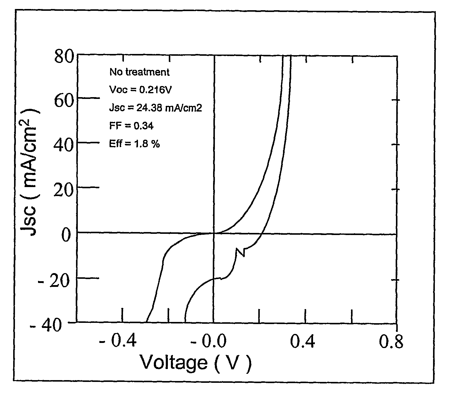
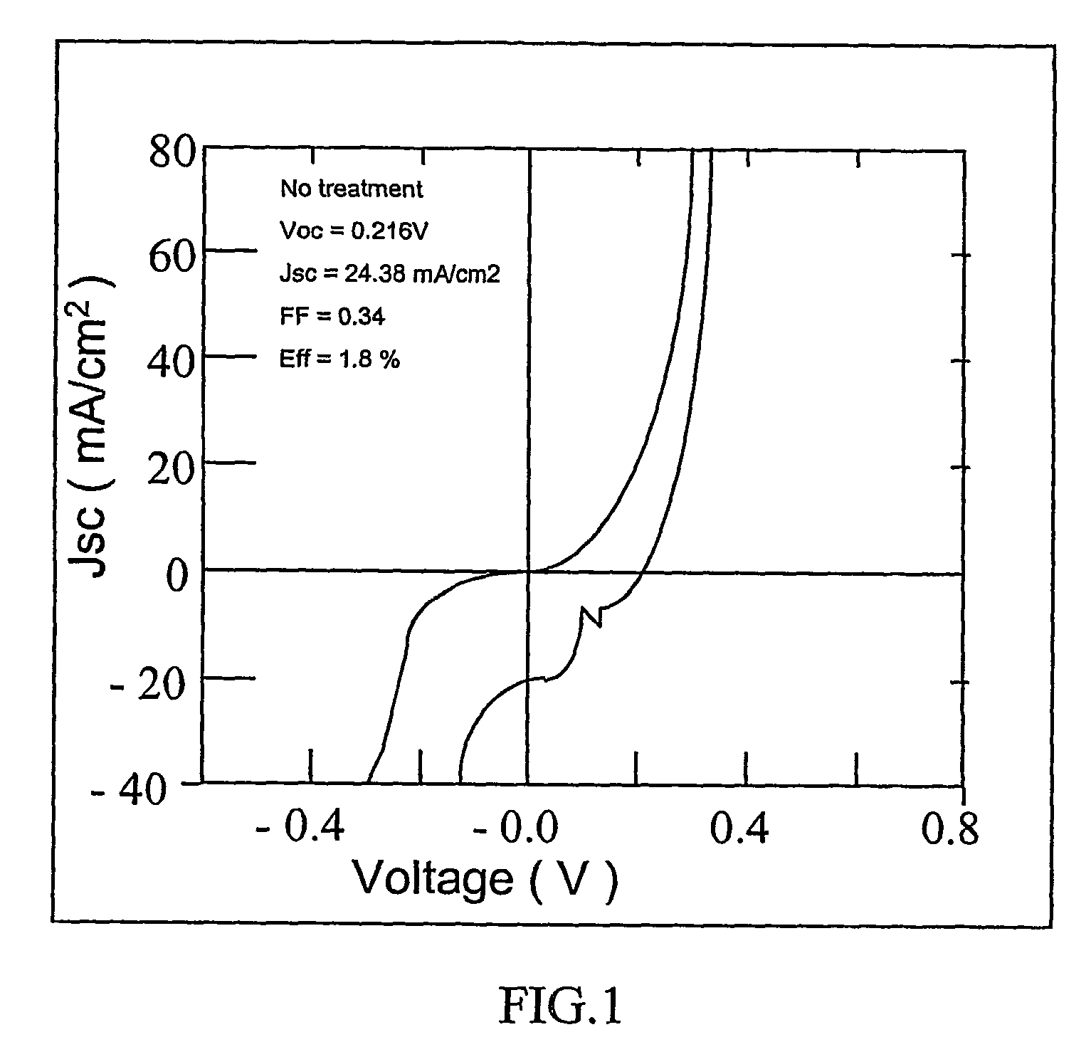
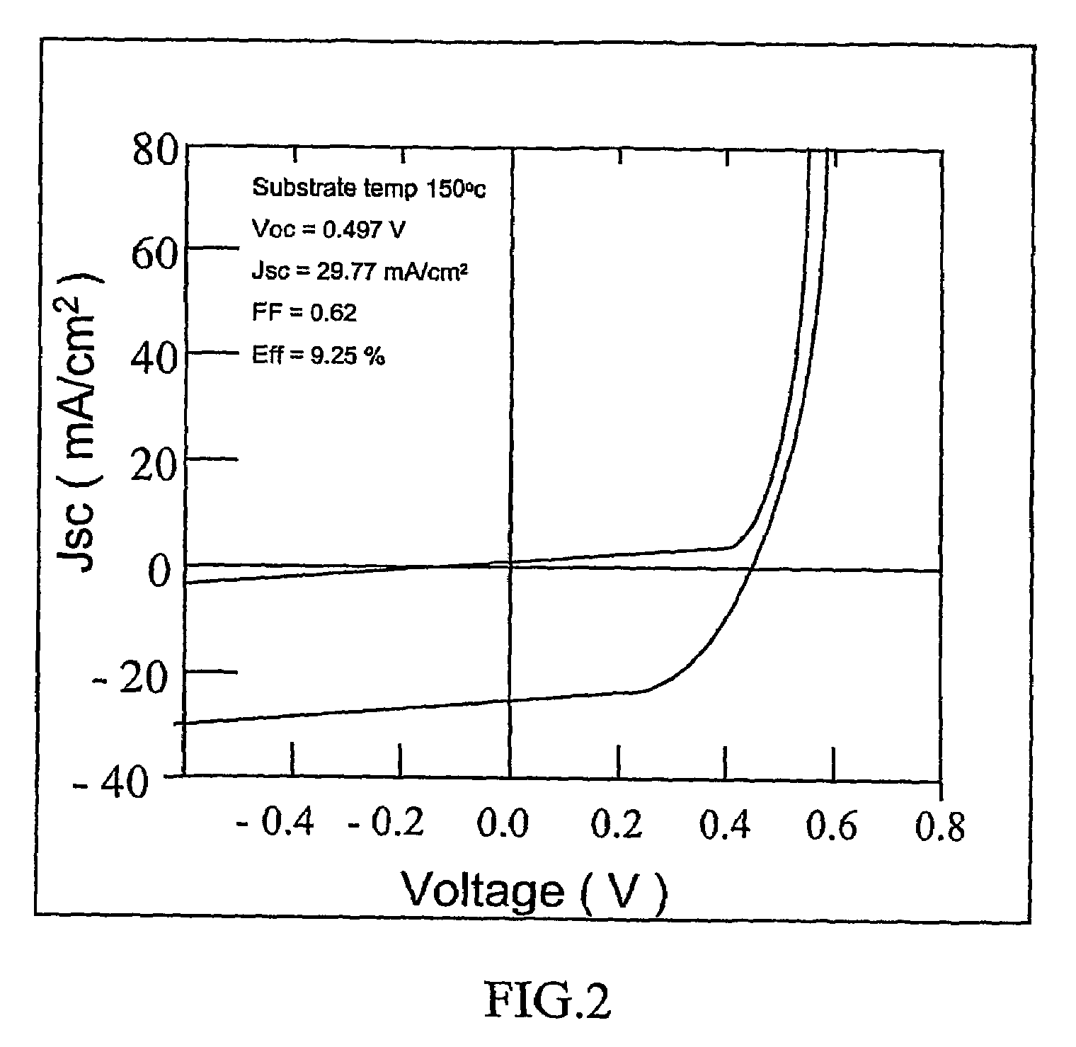
[0027]A co-evaporated CIGS film was divided into four parts, 2″×1″ in length and loaded into a chamber along with a Mo / glass substrate. Zinc acetate dihydrate solid was loaded in a Mo boat. A thermocouple touching the back side of the CIGS substrate was used to control the temperature (Tglass).

[0028]The zinc acetate dihydrate source temperature was raised slowly and the charge was evaporated slowly, while the substrate is brought to the desired temperature before the evaporation is started. The substrate was exposed during the entire time. The exposure time was not controlled, and the evaporation lasted for about 2 to about 4 minutes. The samples were removed and etched in acetic acid in an amount of about 50% by volume in water to remove the ZnO deposit. Sputtered ZnO was deposited next in MRC.

[0029]The graph of FIG. 1 shows a weak diode in the case of no treatment in accordance with the invention process.

[0030]In FIG. 2 where Tg=150° C., and was treated in accordance with the inve...


PUM

PropertyMeasurementUnit
temperatureaaaaaaaaaa

Abstract

A process for making a thin film ZnO / Cu(InGa)Se2 solar cell without depositing a buffer layer and by Zn doping from a vapor phase, comprising: depositing Cu(InGa)Se2 layer on a metal back contact deposited on a glass substrate; heating the Cu(InGa)Se2 layer on the metal back contact on the glass substrate to a temperature range between about 100° C. to about 250° C.; subjecting the heated layer of Cu(InGa)Se2 to an evaporant species from a Zn compound; and sputter depositing ZnO on the Zn compound evaporant species treated layer of Cu(InGa)Se2.

Description

CONTRACTUAL ORIGIN OF THE INVENTION[0001]The United States Government has rights in this invention under Contract No. DE-AC3699GO10093 between the United States Department of Energy and the National Renewable Energy Laboratory, a division of the Midwest Research Institute.TECHNICAL FIELD[0002]The present invention relates to Zinc oxide / Copper Indium Gallium Selenium Disulfide solar cells characterized by conversion efficiencies of >11%. The cells are prepared by subjecting Copper Indium Gallium Disulfide (CuInGaSe2) or CIGS thin films to evaporant species from zinc acetate dihydrate at varying substrate temperatures, and sputter depositing ZnO thereon to provide a transparent electrode for the cell. The innovation of the invention constitutes a basis for in-line junction fabrication processes for preparing CIGS thin films that do not require the use of a Cd compound and requires no buffer layers.BACKGROUND ART[0003]Processes for manufacture of high light to electrical energy conv...

Claims


Application Information

Patent Timeline
Patent Type & Authority Patents(United States)
IPC IPC(8): H01L31/18H01L31/00H01L31/0272H01L31/0336H01L31/04H01L31/072
CPCH01L31/0749H01L31/1836Y02E10/541
Inventor RAMANATHAN, KANNANHASOON, FALAH S.ASHER, SARAH E.DOLAN, JAMESKEANE, JAMES C.
Owner ALLIANCE FOR SUSTAINABLE ENERGY
Why Eureka
Try Eureka