Semiconductor memory device
a memory device and semiconductor technology, applied in the field of semiconductor memory devices, can solve the problems of large cr delay of word lines, and resistance of word lines
- Summary
- Abstract
- Description
- Claims
- Application Information
AI Technical Summary
Benefits of technology
Problems solved by technology
Method used
Image

Examples
embodiment 1
[0042][Embodiment 1]
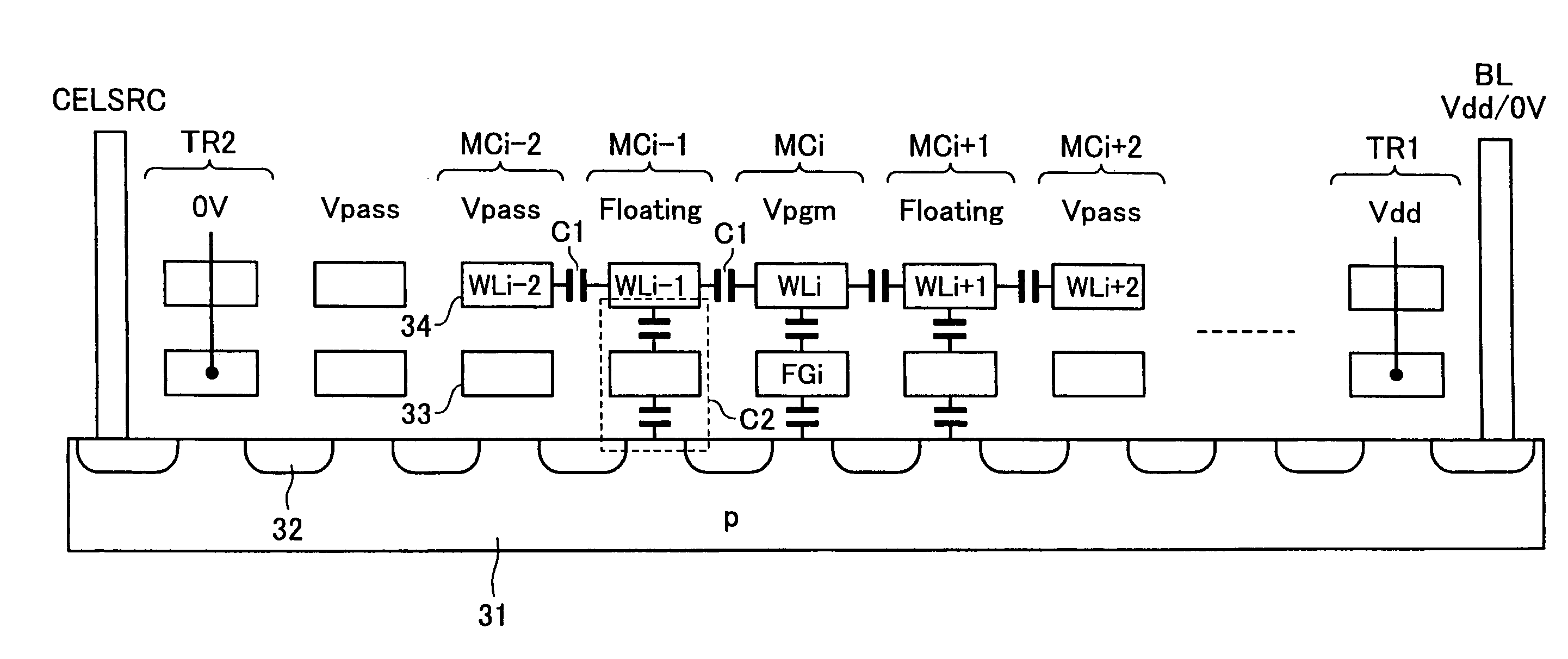
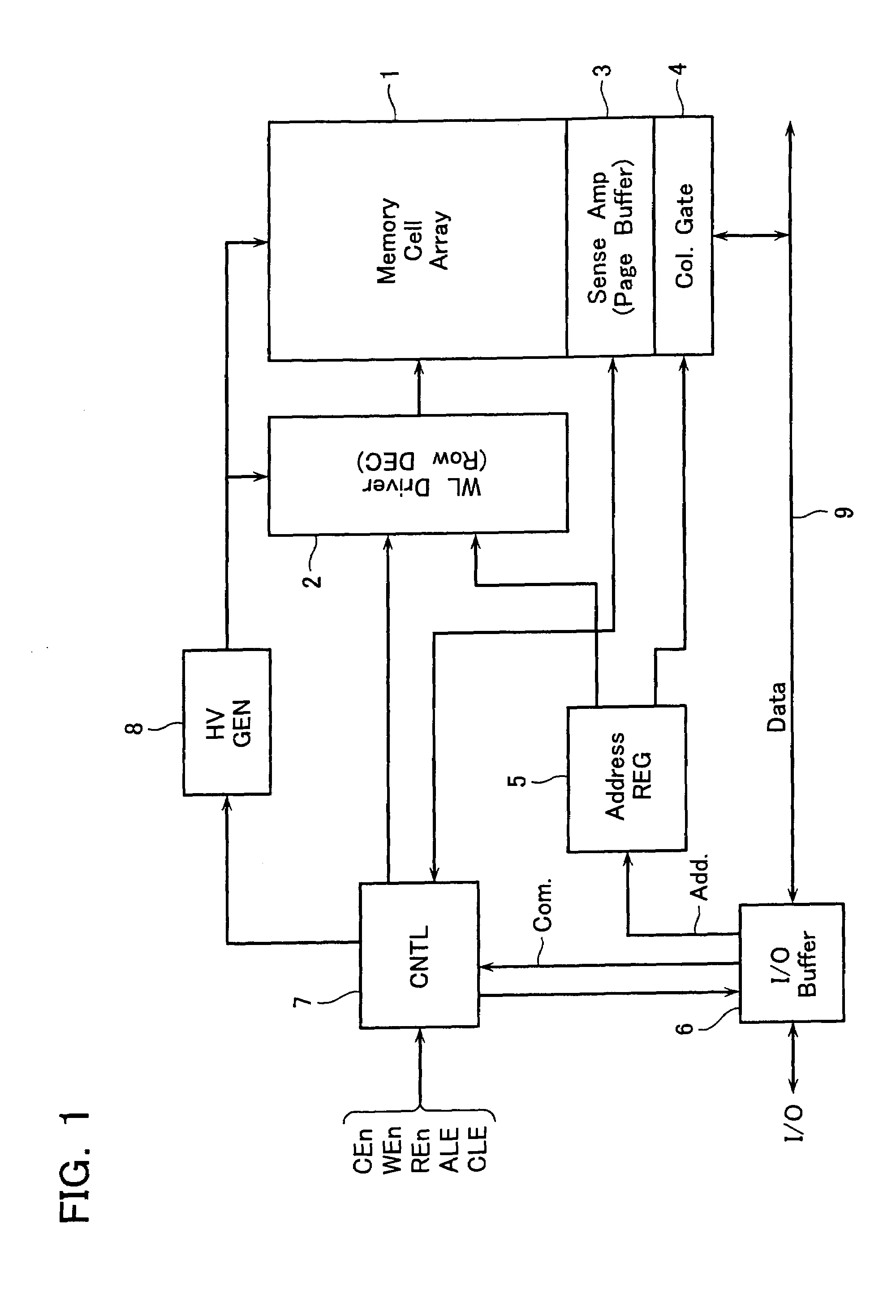
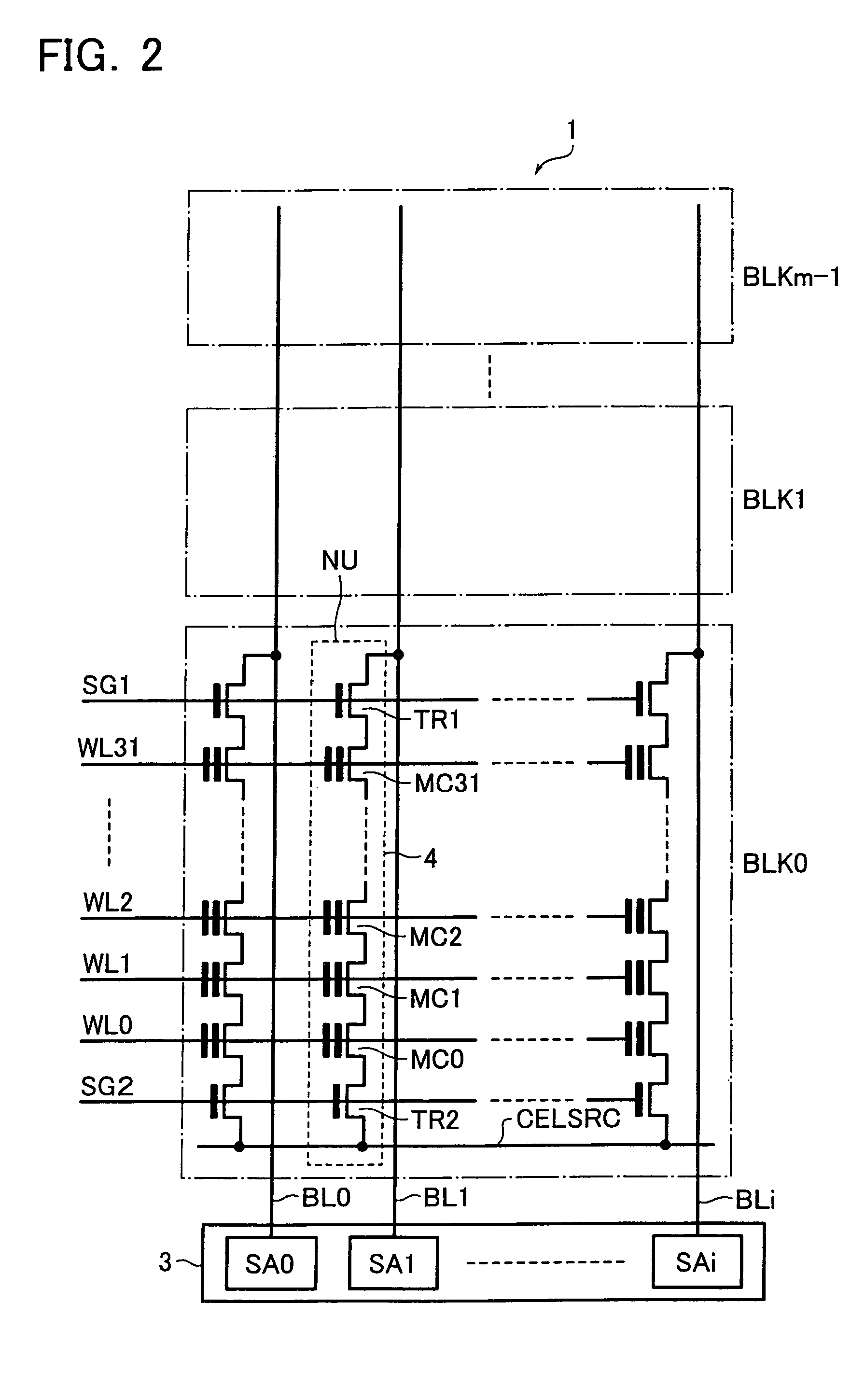
[0043]FIG. 1 shows a functional block configuration of a NAND-type flash memory device, and FIG. 2 shows an arrangement of a memory cell array 1 thereof. These configuration and arrangement may be used common to the entire embodiments as described below. The memory cell array 1 is formed of NAND cell units NU arranged in a matrix manner. One NAND cell unit NU is formed of plural memory cells MC (MC0, MC1, . . . , MC31) connected in series and select gate transistors TR1 and TR2 coupled to the respective ends of the memory cell string. A drain of the select gate transistor TR1 is coupled to a bit line BL, and a source of the select gate transistor TR2 to a common source line CELSRC.
[0044]Control gates of the memory cells MC in one NAND cell unit NU are connected to different word lines WL (WL0, WL1, . . . WL31), respectively. Gates of the select transistors TR1 and TR2 are connected to select gate lines SG1 and SG2, respectively, which are disposed in parallel wit...
embodiment 2
[0074][Embodiment 2]
[0075]FIG. 8 shows a timing chart in accordance with another write operation example different from that shown in FIG. 5. In case of FIG. 5, the adjacent-unselected word lines WLi−1, WLi+1 are boosted in potential only by capacitive coupling from the selected word line WLi. As shown in FIG. 8, in order to boost the adjacent-unselected word lines WLi−1, WLi+1 to be higher than that in the embodiment shown in FIG. 5, it is effective to raise the control signal PUSELFL to be “H” at timing T2 so as to make the adjacent-unselected word lines WLi−1, WLi+1 floating before rising of the write voltage Vpgm.
[0076]For example, giving attention to the adjacent-unselected word line WLi−1 (CGi−1) in case word line WLi (CGi) is selected, it starts to rise up in potential at timing T2 by capacitive coupling from word line WLi−2 (CGi−2) adjacent to WLi−1 (CGi−1), which rises up to Vpass at timing T2. Further, the selected word line WLi (CGi) starts to rise up at timing T3, whereb...
embodiment 3
[0077][Embodiment 3]
[0078]FIG. 9 shows a timing chart in accordance with still another write operation example different from that shown in FIG. 5. It is different from the above-described Embodiment 2 shown in FIG. 8 that the selected word line WLi is also set in a floating state during timings T2–T3 (i.e., from rising of the write pass voltage Vpass to rising of the write voltage Vpgm). This control may be possible by use of AND gate G6 in the word line driver CGDRV shown in FIG. 6. Two inputs of AND gate G6 are page decoder output (CGA) for boosting the selected word line to write voltage Vpgm, and control signal PSELFL, which is used for setting the selected word line in a floating state.
[0079]Making the control signal PSELFL “H” at timing T2, transistor Q3 becomes off prior to outputting the write voltage Vpgm at timing T3. Therefore, the selected word line WLi is set in a floating state from timing T2 to timing T3.
[0080]This Embodiment 3 is effective for improving the electric...
PUM
 Abstract
Description
Claims
Application Information