Method and system for providing spin transfer tunneling magnetic memories utilizing non-planar transistors

a technology of non-planar transistors and magnetic memories, applied in semiconductor devices, digital storage, instruments, etc., can solve the problems of increasing relative transistor leakage power level, difficult to fabricate higher density cells, and general inacceptable power leakag

Active Publication Date: 2008-12-18
SAMSUNG SEMICON
View PDF10 Cites 260 Cited by
  • Summary
  • Abstract
  • Description
  • Claims
  • Application Information

AI Technical Summary

Benefits of technology

[0012]FIG. 3 is a diagram of an exemplary embodiment of a magnetic memory employing the spin transfer effect and non-planar transistors.
[0013]FIGS. 4-24 are diagrams of exemplary embodiments of a magnetic storage cell employing the spin transfer effect and non-planar transistors.
[0014]FIGS. 25-26 are diagrams of exemplary embodiments of magnetic elements used in exemplary embodiments of magnetic storage cells employing the spin transfer effect and non-planar tra

Problems solved by technology

Consequently, it is difficult to fabricate higher density cells 10.
In addition, the relative transistor leakage power level increases as the technology scales down from 0.25 micron to forty-five nm.
For conventional STT-RAM 1 applications, the power leakage

Method used


Image

  • Method and system for providing spin transfer tunneling magnetic memories utilizing non-planar transistors
  • Method and system for providing spin transfer tunneling magnetic memories utilizing non-planar transistors
  • Method and system for providing spin transfer tunneling magnetic memories utilizing non-planar transistors

Examples


Embodiment Construction

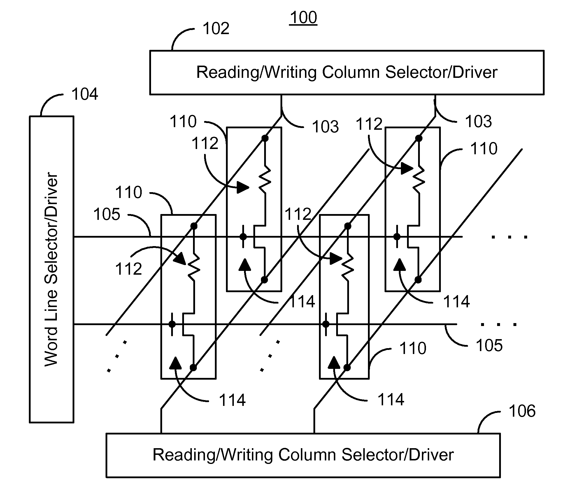
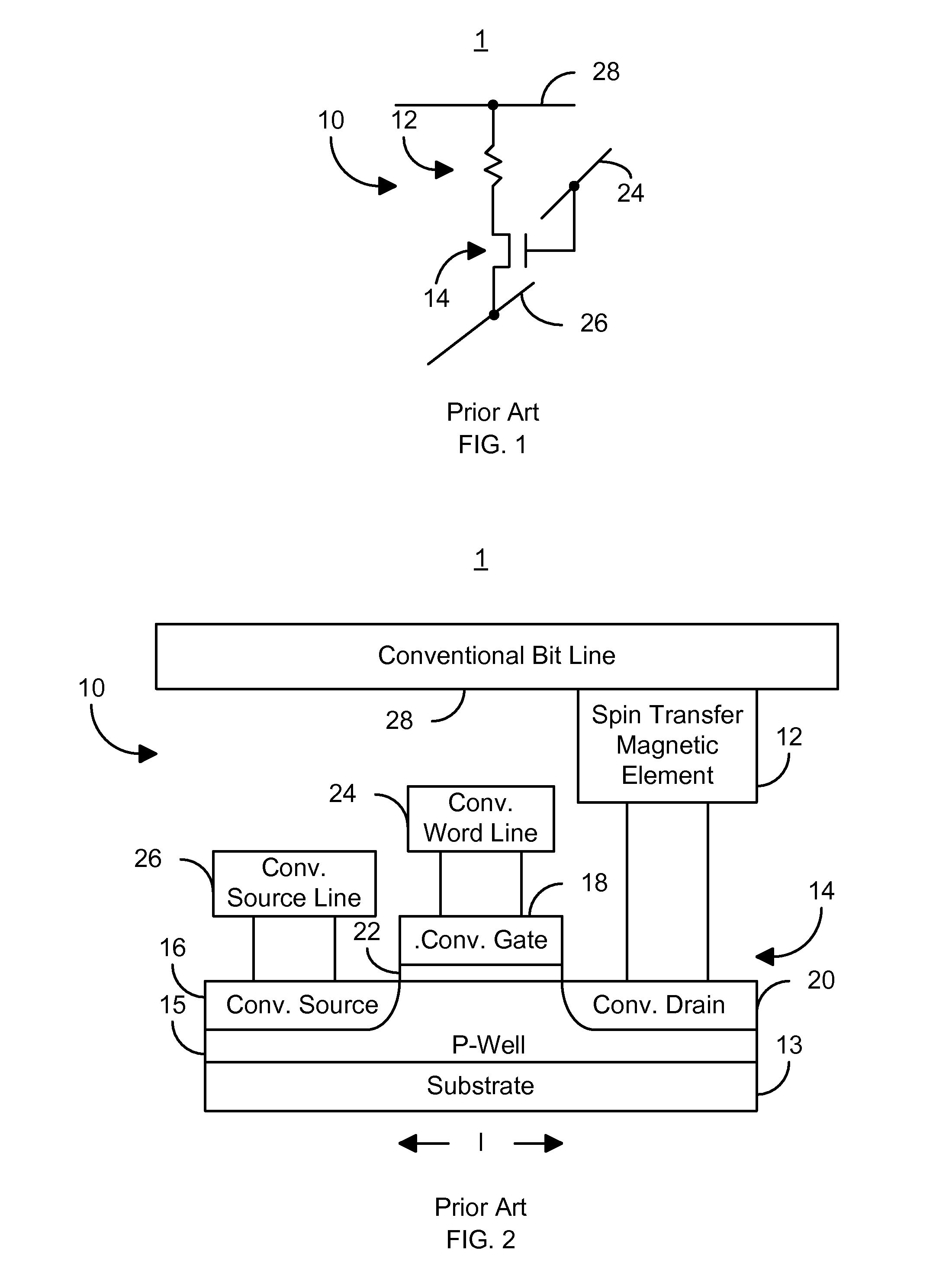
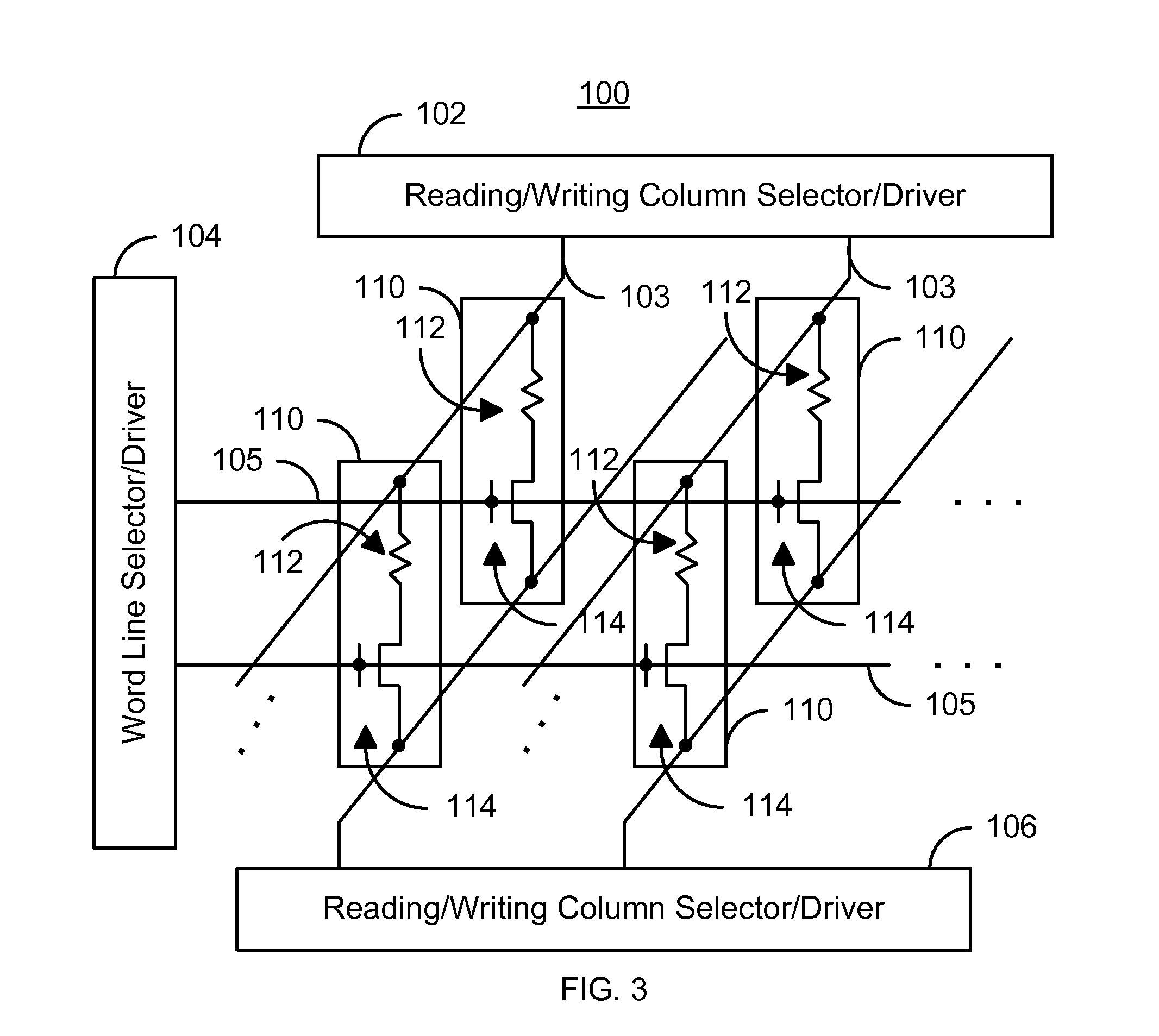
[0018]The present invention relates to magnetic memories. The following description is presented to enable one of ordinary skill in the art to make and use the invention and is provided in the context of a patent application and its requirements. Various modifications to the preferred embodiments and the generic principles and features described herein will be readily apparent to those skilled in the art. Thus, the present invention is not intended to be limited to the embodiments shown, but is to be accorded the widest scope consistent with the principles and features described herein.

[0019]The present invention is mainly described in terms of particular systems provided in particular implementations. However, one of ordinary skill in the art will readily recognize that this method and system will operate effectively in other implementations. For example, the non-planar transistors, magnetic storage cells, magnetic elements, and memories may take a number of different forms. For ex...


PUM


Abstract

A magnetic memory cell and a magnetic memory incorporating the cell are described. The magnetic memory cell includes at least one magnetic element and at least one non-planar selection device. The magnetic element(s) are programmable using write current(s) driven through the magnetic element. The magnetic memory may include a plurality of magnetic storage cells, a plurality of bit lines corresponding to the plurality of magnetic storage cells, and a plurality of source lines corresponding to the plurality of magnetic storage cells.

Description

BACKGROUND OF THE INVENTION[0001]FIGS. 1-2 depict a small portion of a conventional spin transfer torque random access memory (STT-RAM) 1. FIG. 1 depicts a circuit diagram of the portion of the conventional STT-RAM 1, while FIG. 2 depicts a cross-sectional view of the portion of the conventional STT-RAM 1. The conventional STT-RAM 1 includes a conventional magnetic storage cell 10 including a conventional magnetic element 12 and a conventional selection device 14 that is preferably an isolation transistor 14, word line 24, source line 26, and bit line 28. The source line 26 is shown oriented perpendicular to the bit line 28. However, the source line 26 is typically either parallel or perpendicular to the bit line 28, depending on specific architecture used for the conventional STT-RAM 1.[0002]The conventional magnetic element 12 may be a magnetic tunneling junction (MTJ) or other analogous magnetic element and is configured to be changeable between resistance states by driving a cur...

Claims


Application Information

Patent Timeline
IPC IPC(8): G11C11/02G11C11/40H01L21/00
CPCB82Y10/00G11C11/16H01L27/228H01L29/785H01L29/7853H01L29/7854Y10S977/935G11C11/1659G11C11/161G11C11/1675H10B61/22
Inventor CHEN, EUGENEHUAI, YIMINGDRISKILL-SMITH, ALEXANDER A.G.
Owner SAMSUNG SEMICON
Why Eureka
Try Eureka