Display circuit with optical sensor

Inactive Publication Date: 2007-02-27
NOKIA TECHNOLOGLES OY
View PDF21 Cites 96 Cited by
  • Summary
  • Abstract
  • Description
  • Claims
  • Application Information

AI Technical Summary

Benefits of technology

[0016]It is an object of embodiments of the present invention to provide for optical input in combination with a flat-panel display without a significant increase in size and / or weight and / or cost.
[0018]It is an object of embodiments of the present invention to provide for optical input in combination with a display without a significant decrease in the quality of the images on the display.
[0019]Embodiments of the present invention provide circuits in which optical sensors and pixel circuits are integrated on the same substrate. This provides extremely good transparency to the pixel circuits, significantly reduces optical degradation and minimises parallax. It also reduces the size, cost and weight of devices. The use of integrated optical sensors, such as phototransistors, provides high resolution.
[0020]Embodiments of the present invention provide circuits in which optical sensors and pixel circuits are integrated on the same substrate and the control lines used for controlling the pixel circuits are advantageously re-used for controlling the optical sensors. This reduces the complexity of the circuit and allows existing driver hardware to used to drive the circuit with only minor modifications.

Problems solved by technology

Optical scattering against the spacer particles and the glass surface further reduces the image quality of the underlying display.
However, this techniques requires expensive optical components such as lenses, mirrors and transmitters and has a limited resolution.
Another technique detects surface acoustic waves travelling on a thick front glass, but this has limited resolution.
There therefore does not exist any satisfactory circuit which combines optical input with display output.
The existing solutions may require extra components which add size, weight and expense.
The existing solutions also suffer from insufficient resolution and if a touch screen is placed in front of the display it introduces parallax because the input and output planes are not co-planar and it reduces the image quality.

Method used


Image

  • Display circuit with optical sensor
  • Display circuit with optical sensor
  • Display circuit with optical sensor

Examples


Embodiment Construction

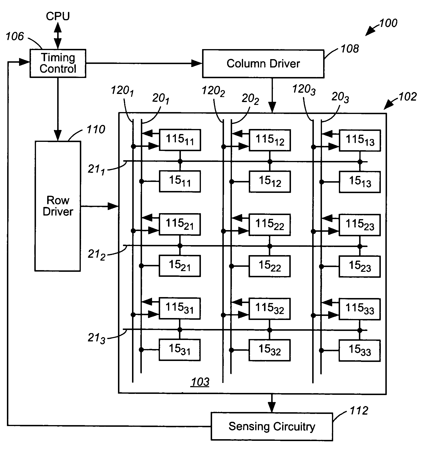
[0029]FIG. 4 illustrates a combined input / output device 100 having an input / output matrix 102 and control circuitry for controlling the input / output matrix. The input / output display matrix comprises a flat-panel display matrix with embedded optical sensors arranged in a matrix.

[0030]The input / output matrix 102 comprises a display matrix of picture element (pixel) circuits, each comprising a pixel integrated on a substrate 103. The display matrix in this example is monochrome and comprises an N row by M column array of picture element (pixel) circuits 15nm, each comprising a pixel. The portion of the display matrix 102 corresponding to n=1, 2 and 3 and m=1, 2 and 3 is illustrated. Each of the N rows of pixel circuits 151m, 152m, 153m . . . 15Nm, where m=1, 2, 3 . . . M, has its own associated row select line 21n integrated on the substrate 103. The row select line 21n is connected to each of the pixel circuits 15n1, 15n2, 15n3 . . . 15nM in its associated row. If the row select line ...


PUM


Abstract

A combined input / output device having a display mode in which it operates as a matrix display and sensing mode in which it receives optical input, comprising multiple picture element circuits arranged as a matrix display and multiple optical sensors arranged as a sensor matrix. The optical sensors and pixel circuits are integrated on the same substrate and the control lines used for controlling the pixel circuits are advantageously re-used for controlling the optical sensors. A plurality of optical sensors are enabled at a time, thereby allowing for the discrimination of inputs by gesture.

Description

CROSS-REFERENCE TO RELATED APPLICATIONS[0001]Not ApplicableBACKGROUND OF THE INVENTION[0002]There exist a number of different input and output devices suitable for use in a human machine interface (HMI). A popular output device is the active matrix flat panel display.[0003]FIG. 1 illustrates a flat-panel display device having a display matrix 2 and control circuitry 4 for controlling the display matrix. The display matrix 2 in this example is monochrome and comprises an N row by M column array of picture element (pixel) circuits 15nm, each comprising a pixel. A colour display is accomplished by dividing each pixel into sub pixels the number of which is the same as they number of primary colours (usually three for red, green, blue, RGB). The portion of the display matrix 2 corresponding to n=1, 2 and 3 and m=1, 2 and 3 is illustrated. Each of the N rows of pixel circuits 151m, 152m, 153m . . . 15Nm, where m=1, 2, 3 . . . M, has an associated row select line 21n. The row select line 2...

Claims


Application Information

Patent Timeline
IPC IPC(8): G09G3/36G02F1/1335G02F1/133G02F1/1362G02F1/1368G06F3/01G06F3/033G06F3/041G09F9/30G09G3/20H01L31/10H01L51/50
CPCG02F1/13338G09G3/20G06F3/0412G02F1/13624G02F2001/13312G09G2360/148G09G2300/08G09G2360/142G06F3/042G02F1/13312
Inventor BERGQUIST, JOHAN
Owner NOKIA TECHNOLOGLES OY
Why Eureka
Try Eureka