High density MIMCAP with a unit repeatable structure

a technology of metal insulation capacitor and repeatable structure, which is applied in the direction of capacitors, semiconductor devices, semiconductor/solid-state device details, etc., can solve the problems of insulator thickness scaling of current materials, affecting the design effect, and affecting the efficiency of conventional silicon based diffusion capacitors. achieve the effect of increasing the surface area

Inactive Publication Date: 2007-03-06
INT BUSINESS MASCH CORP
View PDF13 Cites 23 Cited by
  • Summary
  • Abstract
  • Description
  • Claims
  • Application Information

AI Technical Summary

Problems solved by technology

MIMCAPs are typically fabricated with metal interconnections and do not utilize valuable silicon real estate.
In contrast, a conventional silicon based diffusion capacitor suffers from poor efficiency as internal serial resistance increases, adding an unwanted resistance-capacitance intrinsic delay to the capacitor.
Thus, horizontal plate capacitor structures demand large silicon chip area to form capacitors of needed capacitance.
However, insulator thickness scaling of the current materials has reached a design road block because of the exponential increase in leakage currents, increase in the voltage linearity, and reduction in lifetime reliability which are a consequence of thinner insulating films.
At reduced thicknesses, the capacitance / voltage relationship becomes sufficiently non-linear as to require more complicated circuit designs.
However, deep trench structure MIMCAPs result in high processing costs.
It is also known that some MIMCAP designs, especially those of a vertical MIMCAP structure, require many extra processing steps that are typically not easily integratable into a conventional BEOL process.
For example, the semi-interdigitated MIMCAP design described above does not allow all the nodes of the capacitive plates to couple to one another at all surfaces.
The RIE patterning of these materials is expensive and in some cases requires plasma etching at elevated temperatures and / or a dual step process of plasma or implant damage followed by a wet chemical etch.
This subsequently drives up the manufacturing cost of the MIMCAP capacitor.
Hafnium oxide (HfO2) is an example of a high-k insulating film candidate which is difficult to etch and thus expensive to incorporate into MIMCAP design.

Method used


Image

  • High density MIMCAP with a unit repeatable structure
  • High density MIMCAP with a unit repeatable structure
  • High density MIMCAP with a unit repeatable structure

Examples


Embodiment Construction

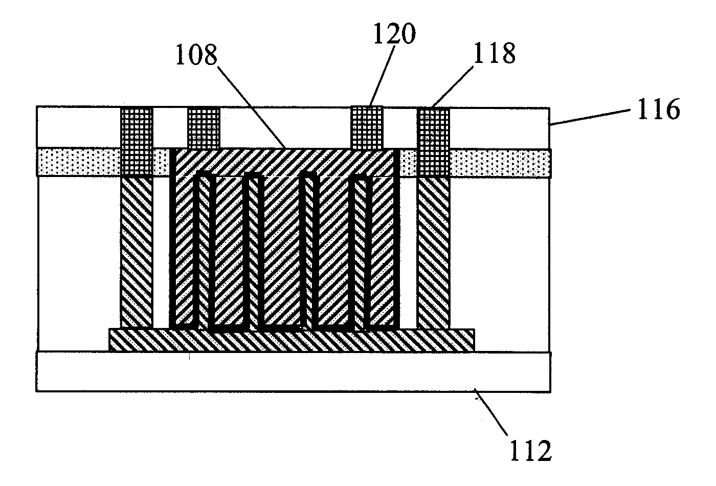
[0025]The invention is directed to a “fully interdigitated MIMCAP structure” and method of manufacture. By using the MIMCAP structure and fabricating process, little surface area is being used for the MIMCAP. In embodiments, the invention also achieves substantial vertical surface capacitive coupling, as well as provides improved mechanical strength to the MIMCAP structure. The structure and method maintain the area of the capacitor despite the loss in horizontal real estate on the semiconductor wafer. Additionally, the structure and method is capable of integrating high-k materials that are difficult to etch by enabling the use of chemical-mechanical polishing (CMP) to define the capacitor dielectric area rather than using RIE.

[0026]In the method and structure, the MIMCAP device dimension scaling is referred to as a “fully interdigitated MIMCAP structure”, e.g., two capacitor node surfaces almost completely coupled to each other mostly in the vertical dimension. The method and stru...


PUM


Abstract

A structure, apparatus and method for utilizing vertically interdigitated electrodes serves to increase the capacitor area surface while maintaining a minimal horizontal foot print. Since capacitance is proportional to the surface area the structure enables continual use of current dielectric materials such as Si3N4 at current thicknesses. In a second embodiment of the interdigitated MIMCAP structure the electrodes are formed in a spiral fashion which serves to increase the physical strength of the MIMCAP. Also included is a spiral shaped capacitor electrode which lends itself to modular design by offering a wide range of discrete capacitive values easily specified by the circuit designer.

Description

BACKGROUND OF INVENTION[0001]1. Field of the Invention[0002]The invention relates to metal-insulator-metal capacitors, and more particularly to a metal-insulator-metal capacitor structure and method of manufacturing a high density of metal-insulator-metal capacitors in a VLSI circuit.[0003]2. Background Description[0004]Metal-insulator-metal capacitors (MIMCAP) are important components in memory, logic and analog circuits. MIMCAPs are typically fabricated with metal interconnections and do not utilize valuable silicon real estate. In contrast, a conventional silicon based diffusion capacitor suffers from poor efficiency as internal serial resistance increases, adding an unwanted resistance-capacitance intrinsic delay to the capacitor.[0005]Horizontal Plate MIMCAP structures having a planar design have been introduced into integrated circuits in the back-end-of-line (BEOL) manufacturing steps. Such BEOL designs require dielectric materials with low processing temperatures to avoid da...

Claims


Application Information

Patent Timeline
Patent Type & Authority Patents(United States)
IPC IPC(8): H01L21/20H01L21/02H01L21/8242H01L23/522
CPCH01L23/5223H01L28/91H01L28/87H01L23/5227H01L2924/0002H01L2924/00
Inventor CHUDZIK, MICHAEL P.HSU, LOUIS L.SHEPARD, JR., JOSEPH F.TONTI, WILLIAM R.
Owner INT BUSINESS MASCH CORP
Why Eureka
Try Eureka