Electron emission device

a technology of electron emission device and spacer, which is applied in the direction of discharge tube main electrode, discharge tube luminescnet screen, discharge tube with screen, etc., can solve the problems of inconvenient installation of spacer, poor productivity, and inability to fix the spacer to predetermined locations in a constant manner, so as to achieve easy and stable installation of spacers

Inactive Publication Date: 2007-03-06
SAMSUNG SDI CO LTD
View PDF7 Cites 18 Cited by
  • Summary
  • Abstract
  • Description
  • Claims
  • Application Information

AI Technical Summary

Benefits of technology

[0012]In accordance with the present invention, an electron emission device is formed with spacer insertion holes at a grid electrode to make spacers installation easy and stable without using an adhesive material.

Problems solved by technology

However, with the electron emission device having the above-structured grid electrode, as the spacers are separately arranged below and above the grid electrode and are internally adhered to the vacuum vessel using an adhesive material, extra time and cost are consumed in installing these spacers, resulting in poor productivity.
Furthermore, with the conventional electron emission device, it is very difficult to attach the spacers to predetermined locations in a constant manner, and the spacers are likely to be displaced from the proper locations, and / or to be inclined.
If the spacers are displaced and / or inclined, the support structure between the first and the second substrates is non-balanced, and is likely to be broken during the exhaust process.
When the adhesive material is partially vaporized during the sealing and exhaust processes while generating gas, it detrimentally affects the vacuum degree, and the vaporized gas needs to be exhausted.

Method used


Image

  • Electron emission device
  • Electron emission device
  • Electron emission device

Examples


Embodiment Construction

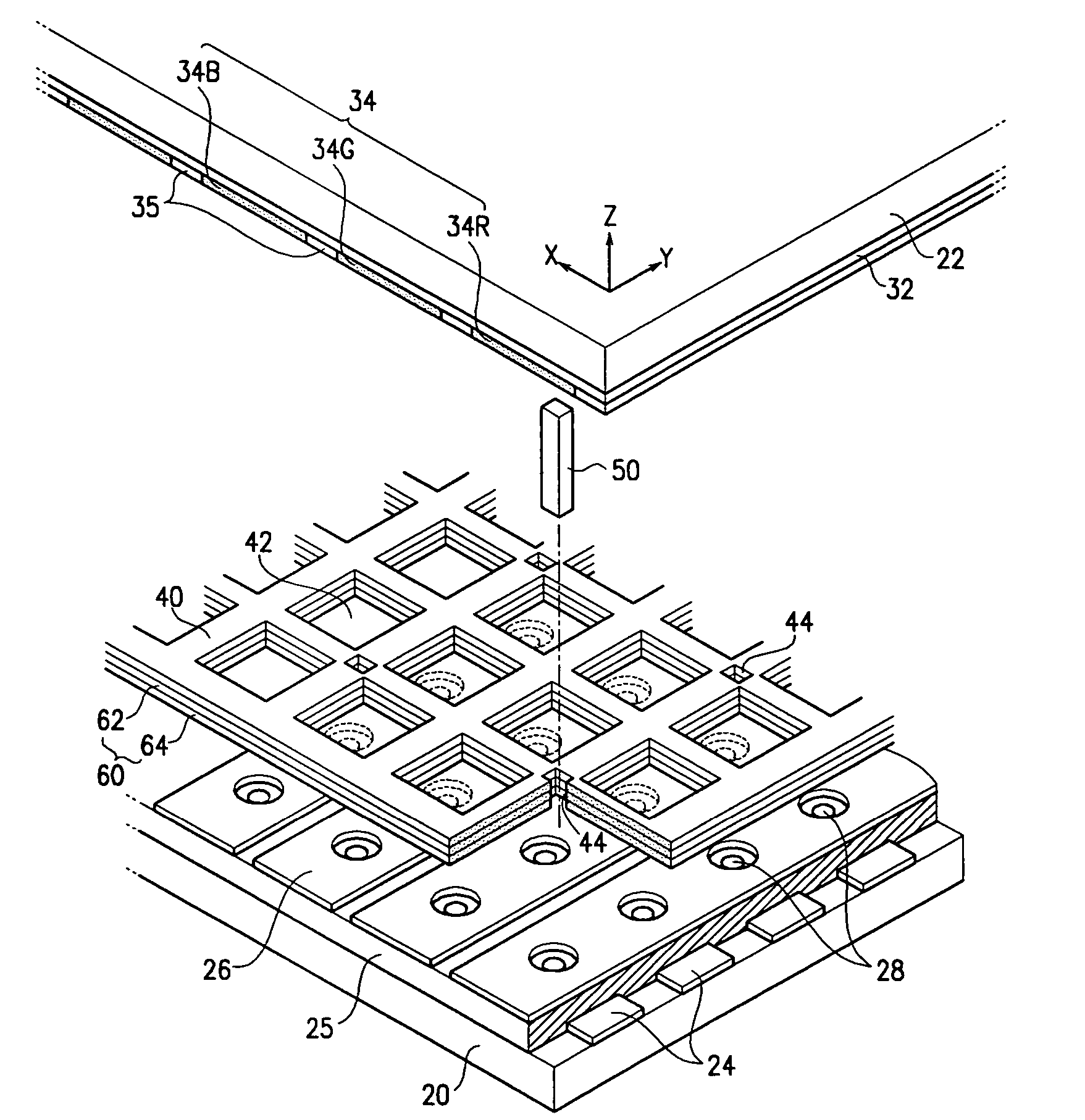
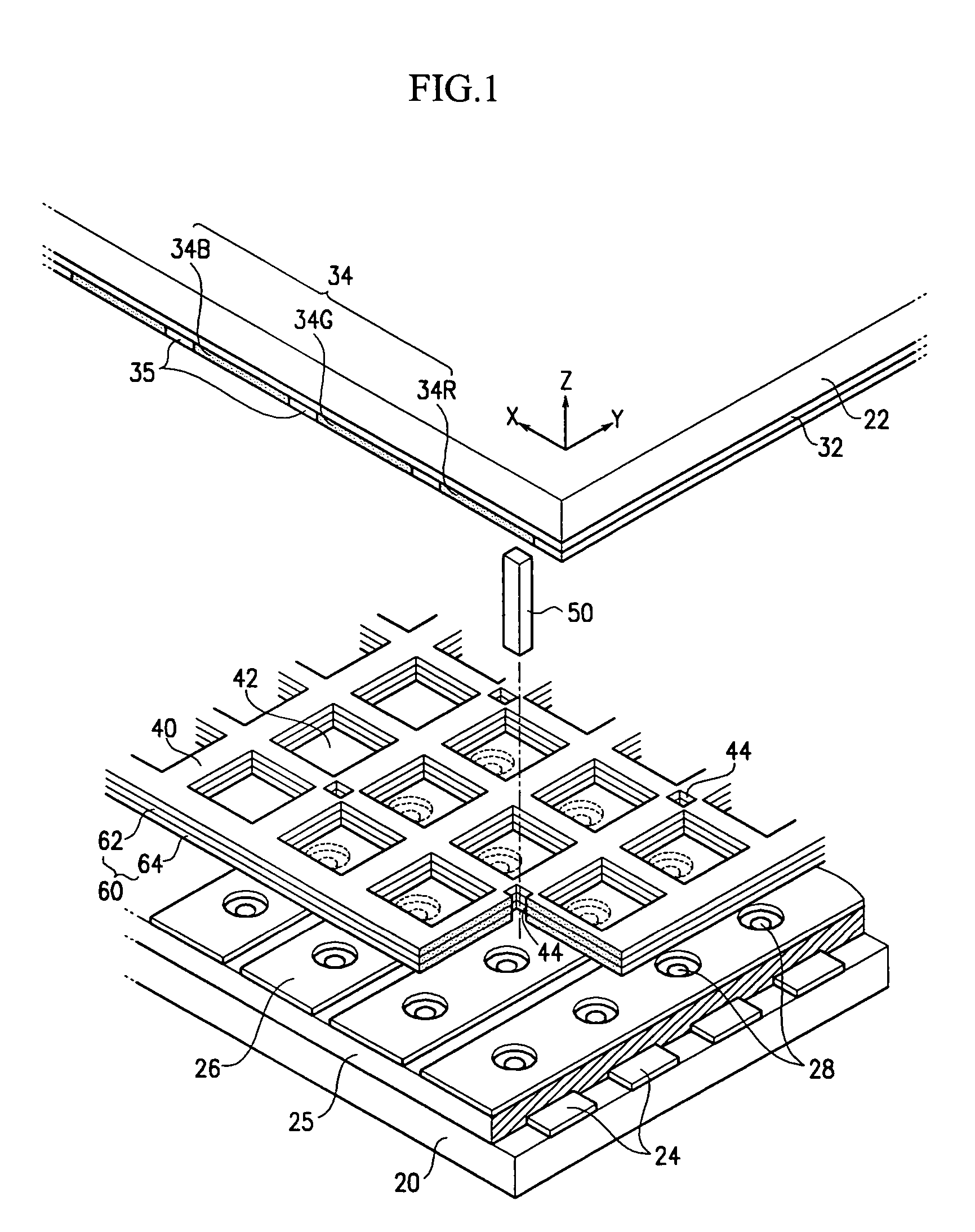
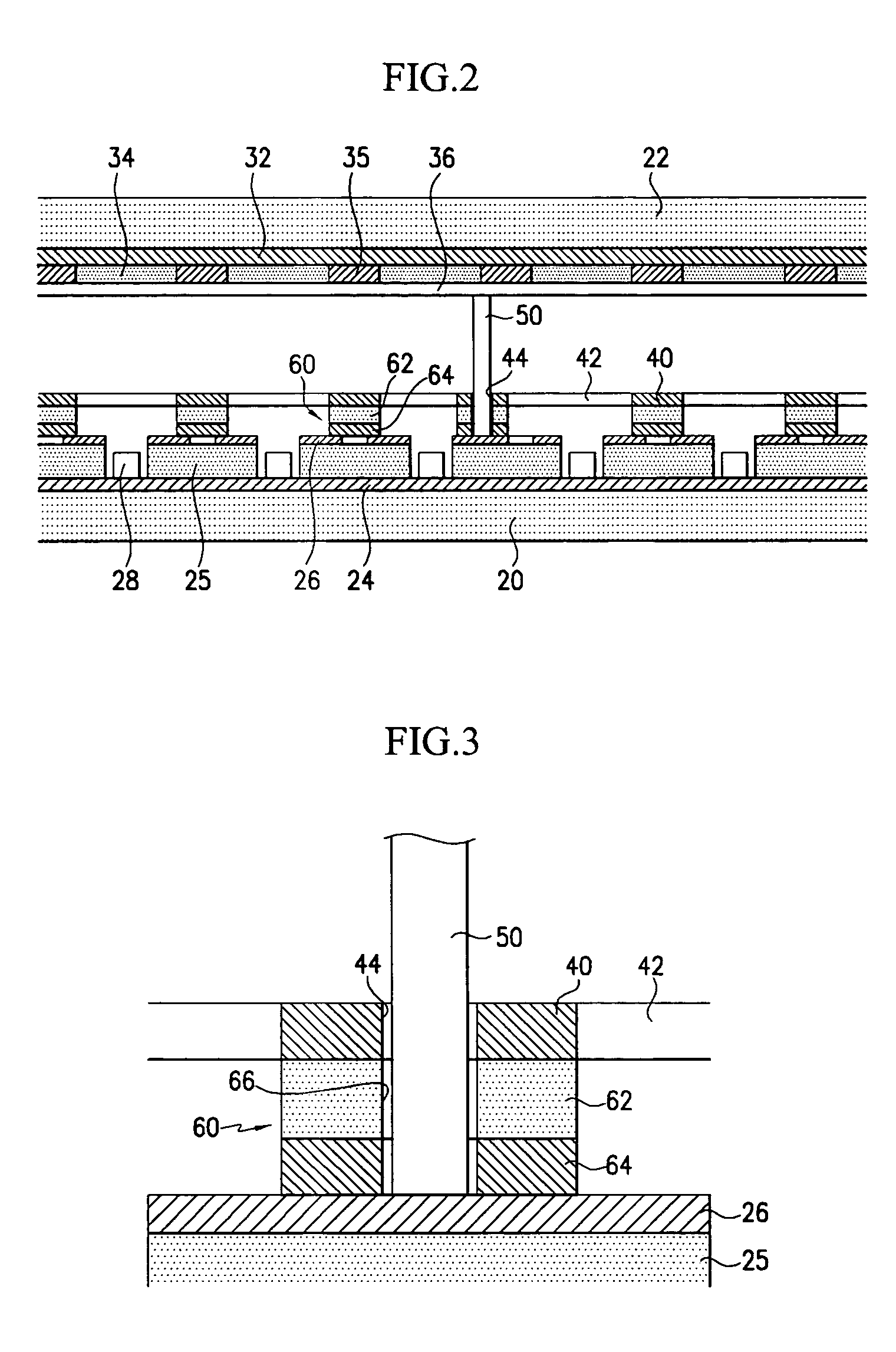
[0032]FIGS. 1 to 3 illustrate an FEA-type of electron emission device, and FIG. 6 illustrates an SCE-type of electron emission device.

[0033]As shown in FIGS. 1 and 2, the electron emission device includes first and second substrates 20, 22 facing each other with a predetermined distance therebetween to form a vacuum vessel. An electron emission unit is provided at the first substrate 20 to emit electrons, and an image display unit is provided at the second substrate 22 to emit light due to the electrons, thereby displaying the desired images.

[0034]The electron emission unit includes a plurality of first electrodes 24 formed on the first substrate 20 as cathode electrodes while being spaced apart from each other by a predetermined distance, and a plurality of second electrodes 26 crossing over the first electrodes 24 as gate electrodes. An insulating layer 25 is interposed between the first electrodes 24 and the second electrodes 26, and electron emission regions 28 are formed on the...


PUM


Abstract

An electron emission display device includes first and second substrates facing each other with a predetermined distance therebetween, an electron emission unit formed at the first substrate, and an image display unit formed at the second substrate. A grid electrode is disposed between the first and the second substrates and has a plurality of beam guide holes arranged in a first predetermined pattern, and spacer insertion holes arranged in a second predetermined pattern. Spacers are inserted into the respective spacer insertion holes of the grid electrode, and are fitted between the first and the second substrates. The size of each of the spacer insertion holes is larger than the outer size of each of the spacers.

Description

CROSS-REFERENCE TO RELATED APPLICATION[0001]This application claims the benefit of and priority to Korean Patent Application No. 10-2004-0045463 filed on Jun. 18, 2004 in the Korean Intellectual Property Office, the entire content of which is incorporated herein by reference.BACKGROUND[0002]1. Field of the Invention[0003]The present invention relates to an electron emission device, and in particular, to an electron emission device having cathode and anode electrodes, and a grid electrode disposed between the cathode and anode electrodes.[0004]2. Description of Related Art[0005]Generally, electron emission devices can be classified into two types. A first type uses a hot cathode as an electron emission source, and a second type uses a cold cathode as the electron emission source. Also, in the second type of electron emission devices, there are a field emission array (FEA) type, a surface conduction emitter (SCE) type, a metal-insulator-metal (MIM) type, a metal-insulator-semiconducto...

Claims


Application Information

Patent Timeline
Patent Type & Authority Patents(United States)
IPC IPC(8): H01J1/88H01J1/00H01J1/62H01J19/42H01J29/46H01J29/86H01J31/12H01J63/04
CPCH01J29/467H01J29/864H01J31/127H01J2329/8665H01J2329/8625H01J2329/863H01J1/30
Inventor SEON, HYEONG-RAE
Owner SAMSUNG SDI CO LTD
Why Eureka
Try Eureka