
High speed configurable transceiver architecture

a transceiver and high-speed technology, applied in the field of data communication, can solve the problems of increasing the amount of processing power of the integrated circuit, increasing the complexity and cost of designing an integrated circuit, and wasting processing power

Active Publication Date: 2007-03-06
XILINX INC
View PDF96 Cites 27 Cited by
  • Summary
  • Abstract
  • Description
  • Claims
  • Application Information

AI Technical Summary

Benefits of technology

[0004]The present invention is an integrated circuit that contains a programmable fabric and a plurality of configurable transceivers located at the peripheral of the programmable fabric. The integrated circuit may contain one or more processor cores. The processor core and the transceivers can be connected by a plurality of signal paths that pass through the programmable fabric.

Problems solved by technology

This increases the amount of processing power of the integrated circuit.
However, the processing power may be wasted if there are insufficient input-output (I / O) resources to transfer data to and from the integrated circuit.
This means that the complexity and costs of designing an integrated circuit also increase.
Further, users also like to use the same integrated circuit to support different applications because of the high costs of learning and using a complicated integrated circuit.

Method used


Image

  • High speed configurable transceiver architecture
  • High speed configurable transceiver architecture
  • High speed configurable transceiver architecture

Examples


Embodiment Construction

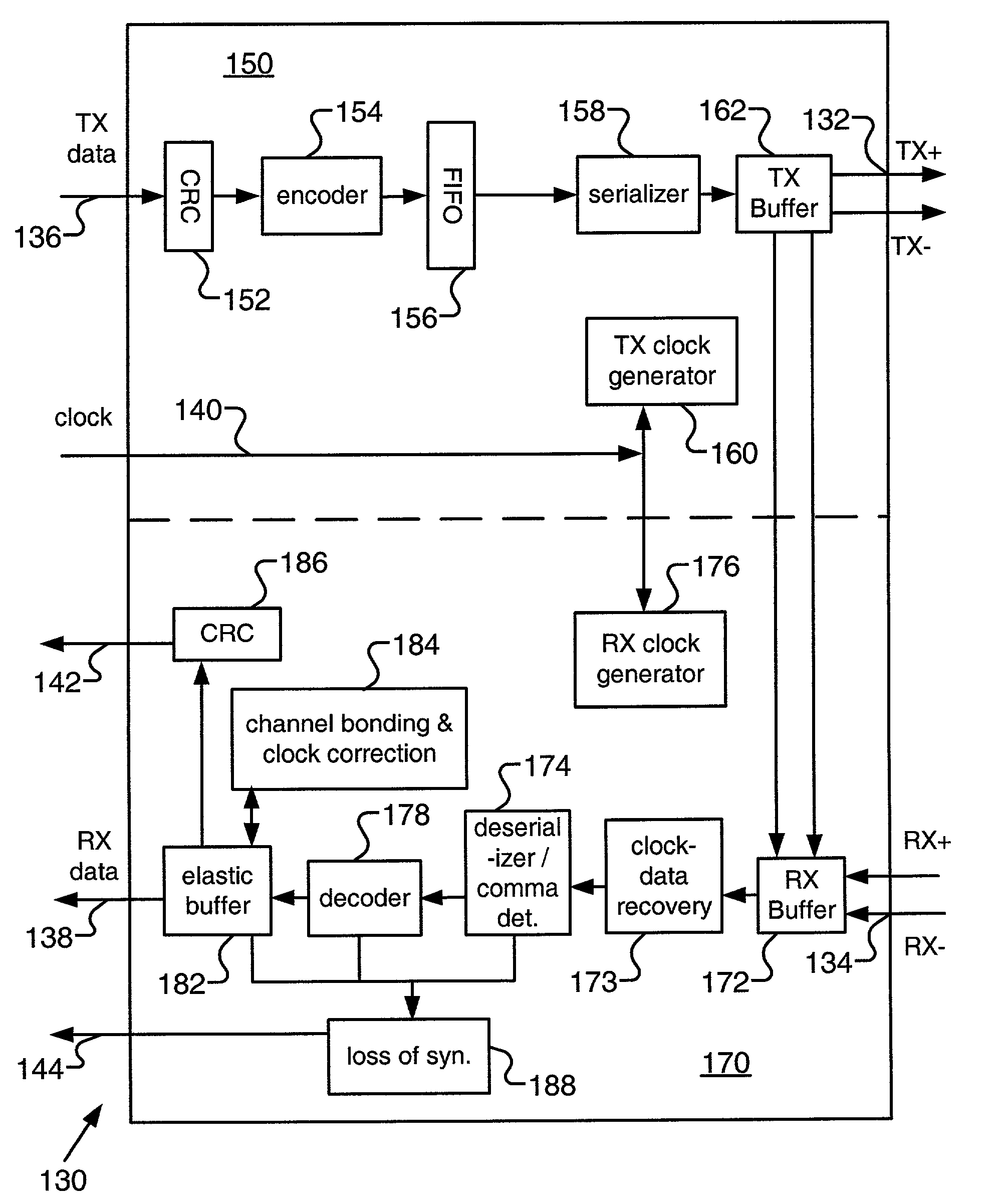
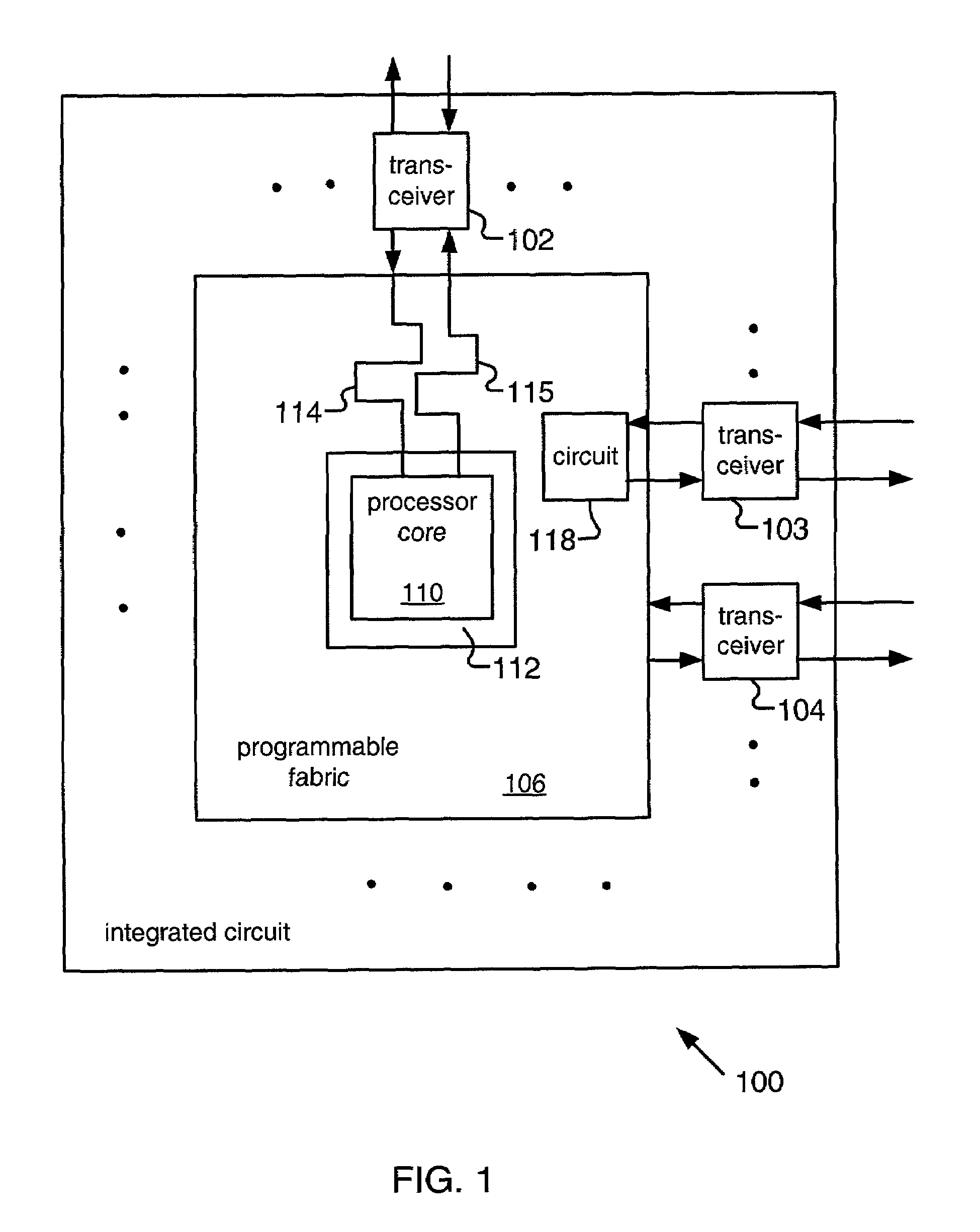
[0010]A schematic diagram showing an integrated circuit 100 of the present invention is shown in FIG. 1. It contains a plurality of transceivers, such as transceiver 102–104, positioned outside of programmable fabric 106. In one embodiment, programmable fabric 106 comprises field programmable gate array (FPGA) fabric. One or more processor cores, such as a processor core 110, can be optionally embedded inside programmable fabric 106. An interface layer 112 is used to facilitate communication between embedded processor core 110 and fabric 106. An example of an interface layer is disclosed in a copending patent application entitled “Programmable Gate Array Having Interconnecting Logic To Support Embedded Fixed Logic Circuitry” (Ser. No. 09 / 968,446 and filed Sep. 28, 2001). Processor core 110 can be connected to one or more transceivers. In FIG. 1, a pair of routed paths 114–115 are used to schematically show the connection from transceiver 102 to processor core 110 through interface l...


PUM


Abstract

One or more configurable transceivers can be fabricated on an integrated circuit. The transceivers contain various components having options that can be configured by turning configuration memory cells on or off. The integrated circuit may also contain programmable fabric. Other components in the transceivers can have options that are controlled by the programmable fabric. The integrated circuit may also contain one or more processor cores. The processor core and the transceivers can be connected by a plurality of signal paths that pass through the programmable fabric.

Description

FIELD OF THE INVENTION[0001]The present invention relates to data communication, and more specifically to a configurable high speed transceiver.BACKGROUND OF THE INVENTION[0002]As a result of improvement in processing technology, it is now possible to put millions of transistors in an integrated circuit. This increases the amount of processing power of the integrated circuit. However, the processing power may be wasted if there are insufficient input-output (I / O) resources to transfer data to and from the integrated circuit. High speed I / O transceivers alleviate this problem by increasing the data transfer speed of the I / O resources. In order to improve performance, circuit designers have started to integrate high speed transceivers into integrated circuits.[0003]Another effect of the increase in the number of transistors is that it is possible to place more circuits in an integrated circuit. This means that the complexity and costs of designing an integrated circuit also increase. ...

Claims


Application Information

Patent Timeline
Patent Type & Authority Patents(United States)
IPC IPC(8): H04B1/38H04L5/16H03K19/173G06F15/78H03M13/15
CPCG06F15/7867
Inventor MENON, SURESH M.GHIA, ATUL V.CORY, WARREN E.SASAKI, PAUL T.FREIDIN, PHILIP M.ASUNCION, SANTIAGO G.COSTELLO, PHILIP D.VADI, VASISHT M.BEKELE, ADEBABAY M.VERMA, HARE K.
Owner XILINX INC
Learn More