Organic electroluminescent device employing multi-layered anode

Active Publication Date: 2007-03-13
SAMSUNG DISPLAY CO LTD
View PDF15 Cites 52 Cited by
  • Summary
  • Abstract
  • Description
  • Claims
  • Application Information

AI Technical Summary

Benefits of technology

[0015]To overcome the problems, the present invention provides a front-emitting organic EL device with improved emissio

Problems solved by technology

Such a reduction in aperture ratio increases current density, which may adversely affect performance of an organic EL device.
The use of Al for forming an anode greatly increases a driving voltage, making it difficult to be used in an organic EL device in practice.
Pure R, G and B color emissions produced from such a structure are subjected to multiple interference due to partial reflectance occurring at the semi-transparent anode.
The use of the single metal layer as an anode reduces the reflectivity of the anode to less than 60%, deteriorating a utilization efficiency of emitted light, resulting in a rise in

Method used


Image

  • Organic electroluminescent device employing multi-layered anode
  • Organic electroluminescent device employing multi-layered anode
  • Organic electroluminescent device employing multi-layered anode

Examples


example 1

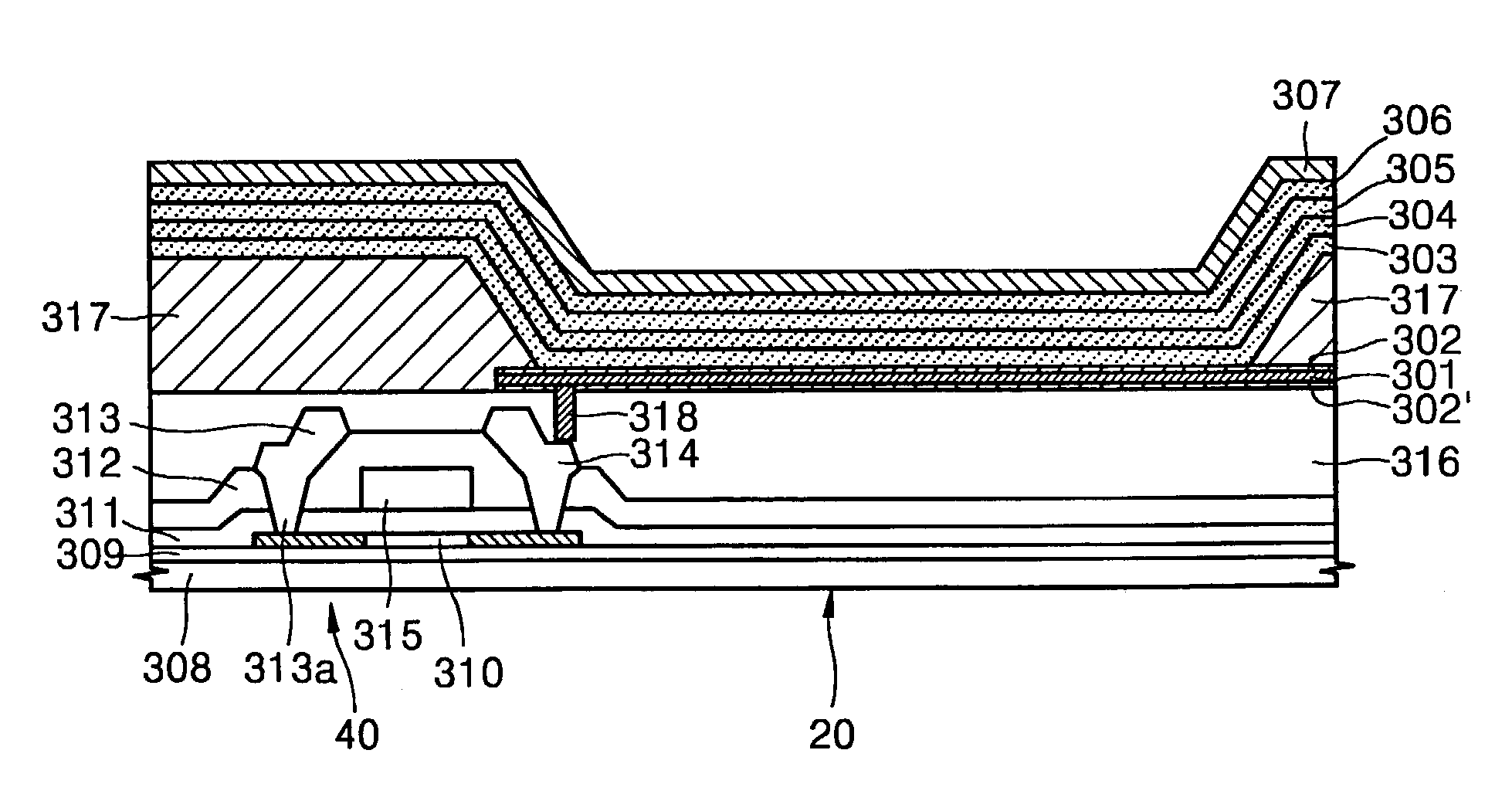
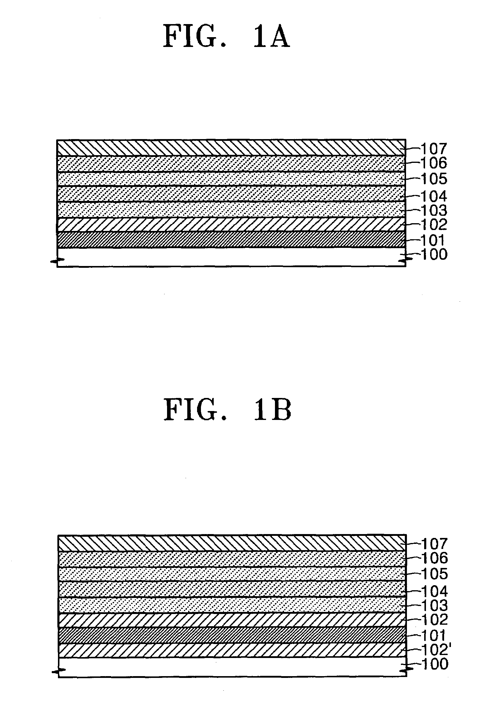
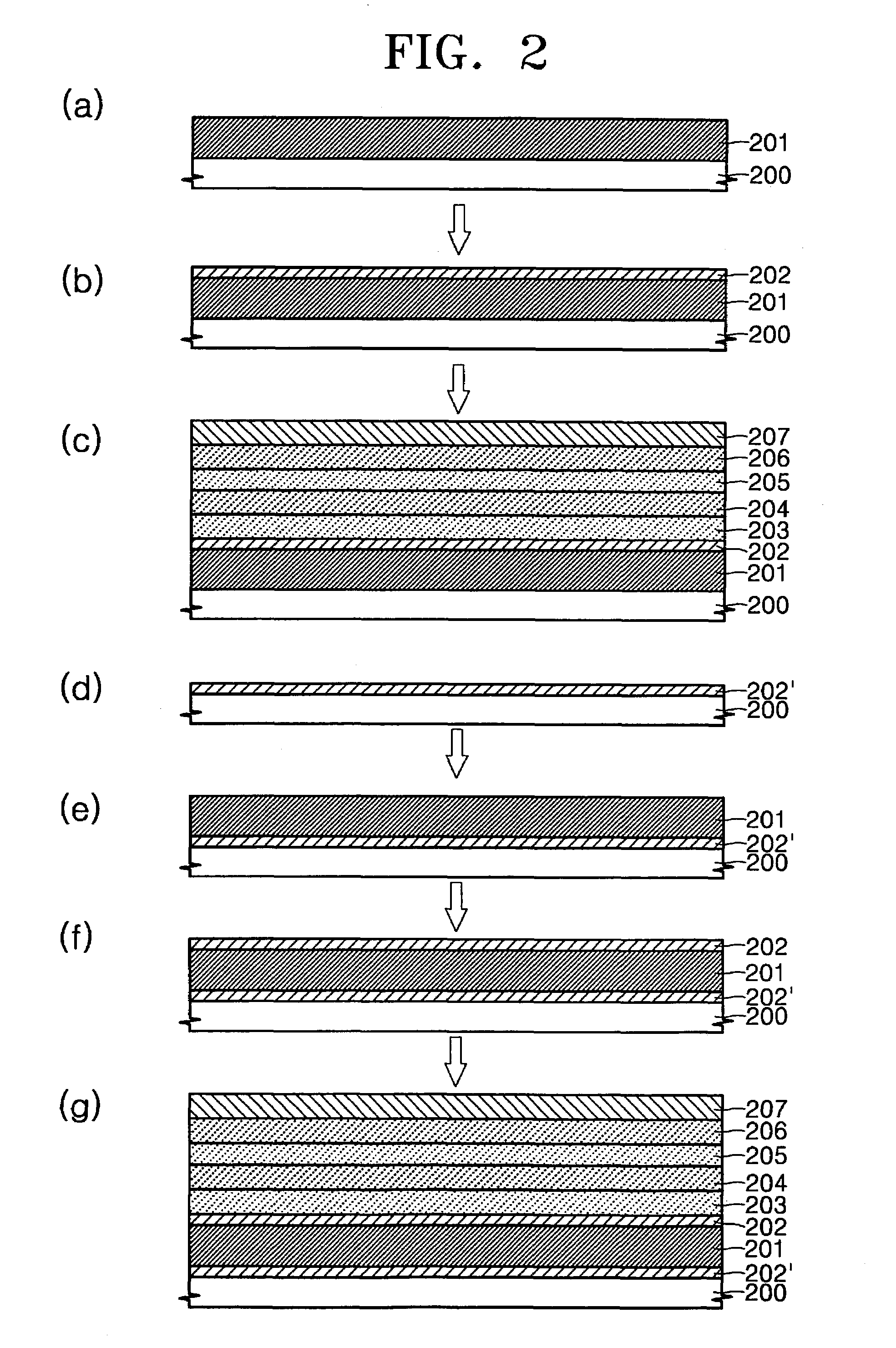
[0094]Ni was sputtered onto a glass substrate to a thickness of 75 Å at 0.7 KW under 2 mmtorr using an RF sputter to form a third anode. Then Al was sputtered onto the third anode at 4 KW under 4 mmtorr using a DC sputter to form a first anode having a thickness of 1800 Å. Ni was sputtered onto the first anode to a thickness of 75 Å at 0.7 KW under 2 mmtorr using an RF sputter to form a second anode.

[0095]Subsequently, an aqueous solution of HCl was sprayed onto the resultant product as an Al etchant, followed by simultaneous etching at 40° C., thereby forming a patterned anode.

[0096]In order to form an insulator layer on the patterned anode, a 2 mm×2 mm emission area pattern was formed. Subsequently, the resultant product was cleaned using water, isopropyl alcohol and acetone, respectively, and was further cleaned using an UV / O3 cleaner.

[0097]Thereafter, IDE 406 (manufactured by IDEMITSU KOSAN LTD.) was vacuum-deposited on the second anode of the resultant product to form a hole in...

example 2

[0102]The same procedure as Example 1 was performed, except that a thickness of a third anode was 100 Å, a thickness of a second anode was 1800 Å, and a thickness of a first anode was 100 Å, thus completing a front-emitting organic EL device.

example 3

[0103]Al was sputtered onto a glass substrate to a thickness of 1800 Å at 4 KW under 4 mmtorr using a DC sputter to form a first anode. Then, Ni was sputtered onto the third anode at 0.7 KW under 2 mmtorr using an RF sputter to form a second anode having a thickness of 75 Å, thus forming a bilayer anode. Thereafter, the same procedure as Example 1 was performed, thus completing a front-emitting organic EL device.


PUM


Abstract

An organic electroluminescent (EL) device includes a substrate, a first anode formed on the substrate with a reflectivity of 60% or higher, a second anode formed on the first anode, wherein the second anode includes a conductive metal or an oxide thereof having a work function of 4.3 to 5.8 eV, an organic layer formed on the second anode, and a cathode formed on the organic layer.

Description

CROSS-REFERENCE TO RELATED APPLICATIONS[0001]This application claims the benefit of Korean Patent Application No. 2002-35137 filed Jun. 22, 2002, in the Korean Intellectual Property Office, the disclosure of which is incorporated herein by reference.BACKGROUND OF THE INVENTION[0002]1. Field of the Invention[0003]The present invention relates to an organic electroluminescent (EL) device employing a multi-layered anode, and more particularly, to an organic EL device having improved emission efficiency by employing a multi-layered anode having good reflectivity and high hole injecting efficiency.[0004]2. Description of the Related Art[0005]An organic EL device is generally constructed such that a hole injection electrode is arranged on a substrate, e.g., a glass substrate, organic layers for emitting light are stacked on the hole injection electrode, and an electron injection electrode is stacked on the organic layers. An active matrix (AM) drive type organic EL device is constructed s...

Claims


Application Information

Patent Timeline
IPC IPC(8): H05B33/22H01L51/50H05B33/24H05B33/26H05B33/00H01L27/32H01L51/52
CPCH01L51/5206H01L27/3244H01L2251/5315H01L51/5262H10K59/12H10K50/818H10K50/85H10K2102/3026H05B33/26
Inventor LEE, KWANHEESHIN, HYUNEOKCHOI, YONGJOONGKWON, JANGHYUKJUNG, JINWOUNG
Owner SAMSUNG DISPLAY CO LTD
Why Eureka
Try Eureka