GaN based semiconductor light emitting device and method of making the same

a technology of light-emitting devices and semiconductors, which is applied in the direction of semiconductor devices, basic electric elements, electrical equipment, etc., can solve the problem of having to form even thin film layers, and achieve the effect of increasing emission efficiency

Inactive Publication Date: 2005-03-17
TOYODA GOSEI CO LTD
View PDF3 Cites 68 Cited by
  • Summary
  • Abstract
  • Description
  • Claims
  • Application Information

AI Technical Summary

Benefits of technology

[0007] It is an object of the invention to provide a GaN based semiconductor light emitting device that has increased emission efficiency.
[0008] It is a further object of the invention to provide a method of making the GaN based semiconductor light emitting device that has increased emission efficiency, under simplified growth conditions.

Problems solved by technology

Thus, the uneven thin film layer has to be formed under the limited growth conditions.

Method used


Image

  • GaN based semiconductor light emitting device and method of making the same
  • GaN based semiconductor light emitting device and method of making the same
  • GaN based semiconductor light emitting device and method of making the same

Examples


Embodiment Construction

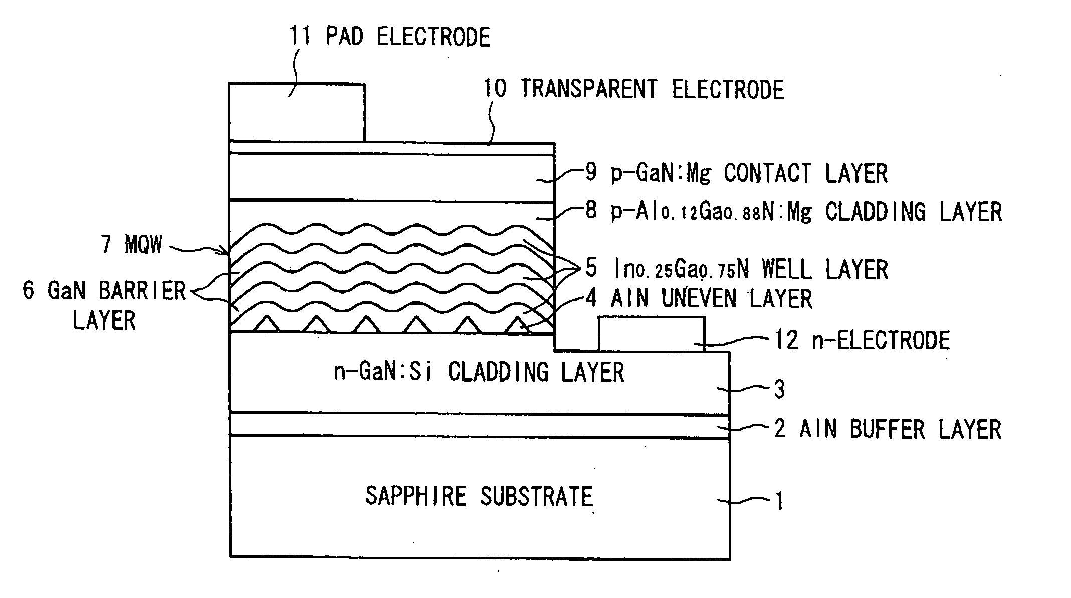
[0029]FIG. 1 is a schematic cross sectional view showing a GaN based semiconductor light emitting device in the preferred embodiment according to the invention.

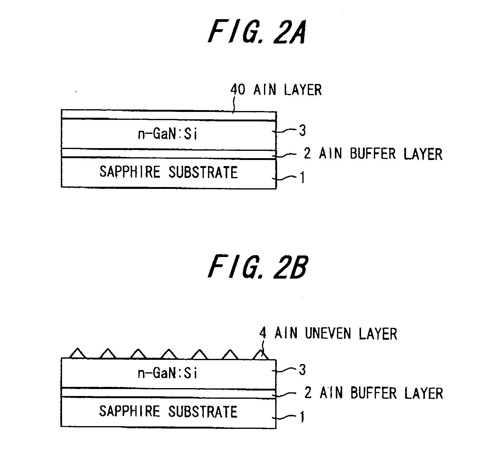
[0030] In the GaN based semiconductor light emitting device, an AlN buffer layer 2 is formed on a sapphire substrate 1 in low temperature growth. On the buffer layer 2, n-type GaN:Si-doped cladding layer (which also functions as a contact layer) 3 is formed. On the n-GaN cladding layer 3, the AlN uneven layer 4 is formed. On the AlN uneven layer 4, MQW (=multiquantum well structure) 7 is formed that is provided with three uneven-formed In0.25Ga0.75N well layers 5 and two uneven-formed GaN barrier layers 6 which are alternately disposed. On the MQW 7, a Mg-doped p-type Al0.12Ga0.88N cladding layer 8 is formed. On the p-cladding layer 8, a M-doped p-type GaN contact layer 9 is formed. By etching part of the p-GaN contact layer 9, p-Al0.12Ga0.88N cladding layer 8, MQW 7 and n-GaN cladding layer 3, a partial surface of the n-GaN...


PUM


Abstract

A GaN based semiconductor light emitting device has: an active layer disposed between an n-type layer and a p-type layer; and a polycrystalline nitride based semiconductor uneven layer disposed between the n-type layer and the active layer. The active layer is formed uneven according to the uneven form of the polycrystalline nitride based semiconductor uneven layer.

Description

[0001] The present application is based on Japanese patent application No.2003-324571, the entire contents of which are incorporated herein by reference. BACKGROUND OF THE INVENTION [0002] 1. Field of the Invention [0003] The invention relates to a GaN based semiconductor light emitting device, and particularly relates to a GaN based semiconductor light emitting device that the emission efficiency can be increased, and a method of making the same. [0004] 2. Description of the Related Art [0005] Japanese patent application laid-open No.10-215029 discloses a GaN based semiconductor light emitting device that is provided with: a thin film layer that is formed uneven on a nitride semiconductor layer under the conditions that the lattice constant mismatch of the thin film layer to the nitride semiconductor layer is ±3% or greater and the thickness of the thin film layer is 50 Å or less; and an active layer that is of nitride semiconductor including indium. In this structure, the active l...

Claims


Application Information

Patent Timeline
Patent Type & Authority Applications(United States)
IPC IPC(8): H01L21/00H01L21/205H01L33/06H01L33/22H01L33/24H01L33/32
CPCH01L33/18H01L33/32H01L33/24
Inventor TAKI, TETSUYA
Owner TOYODA GOSEI CO LTD
Why Eureka
Try Eureka