Structure and method of applying stresses to PFET and NFET transistor channels for improved performance

a technology of pfet and nfet transistors, applied in the direction of transistors, electrical equipment, semiconductor devices, etc., can solve problems such as the reduction of drive curren

Inactive Publication Date: 2007-03-20
CHARTERED SEMICONDUCTOR MANUFACTURING +1
View PDF80 Cites 37 Cited by
  • Summary
  • Abstract
  • Description
  • Claims
  • Application Information

AI Technical Summary

Problems solved by technology

However, if the same compressive stress is applied to the conduction channel of an NFET, its drive current decreases.

Method used


Image

  • Structure and method of applying stresses to PFET and NFET transistor channels for improved performance
  • Structure and method of applying stresses to PFET and NFET transistor channels for improved performance
  • Structure and method of applying stresses to PFET and NFET transistor channels for improved performance

Examples


Embodiment Construction

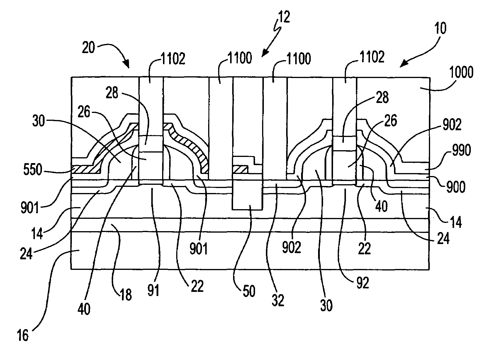
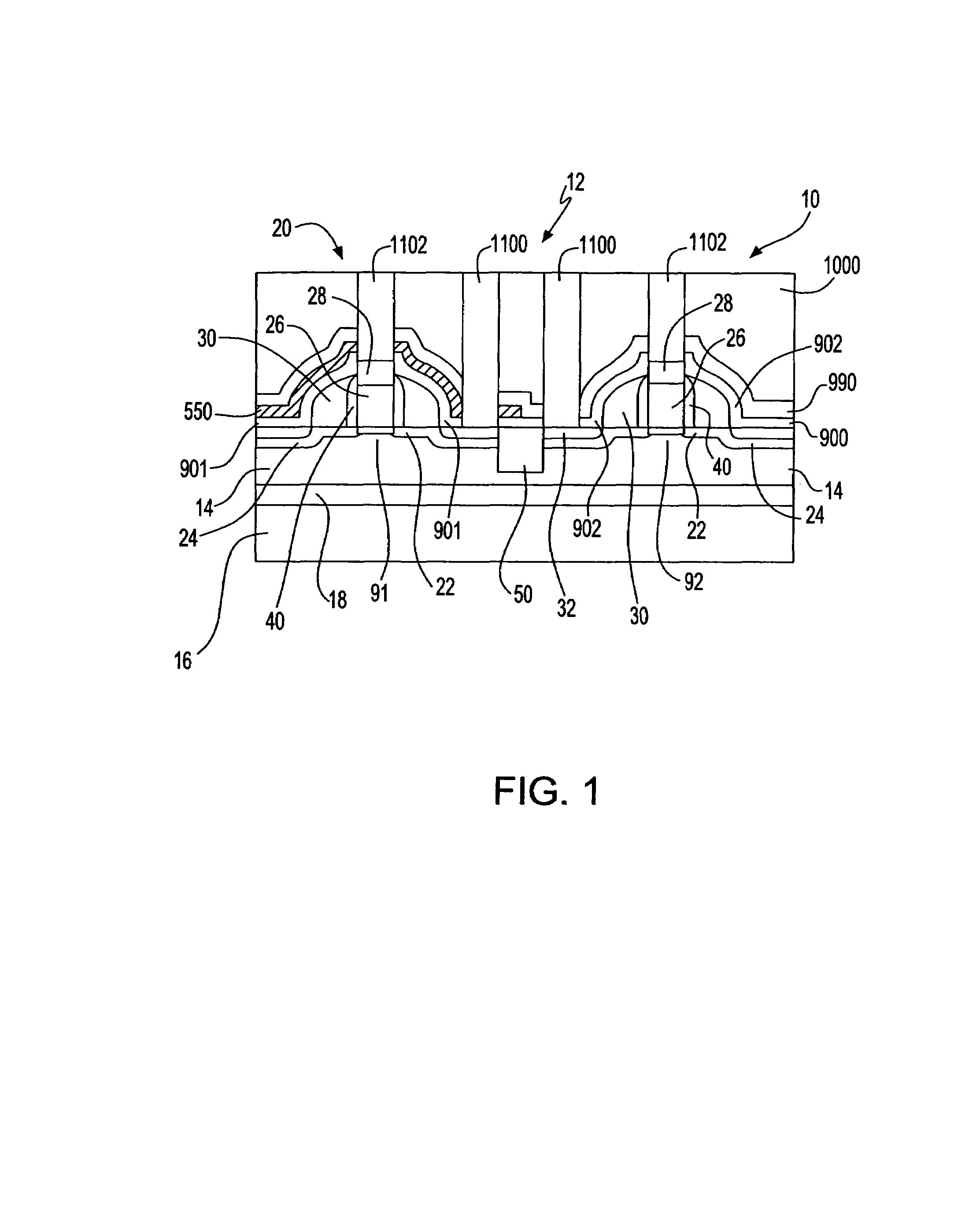
[0008]FIG. 1 is a cross-sectional view illustrating one embodiment of the present invention. As shown in FIG. 1, a single-crystal semiconductor region 14 is illustrated in which two semiconductor devices are provided, such as NFET 10 and PFET 20 of complementary metal oxide semiconductor (CMOS) circuitry. The NFET and PFET are separated by shallow trench isolation (STI) region 50. As discussed earlier, an appropriate stress applied to a transistor channel region can significantly increase carrier mobility, resulting in improved performance. As shown in FIG. 1, a unitary stressed film 900 is disposed over both the PFET 20 and the NFET 10 to impart stresses to each transistor.

[0009]In the exemplary structure shown in FIG. 1, the unitary stressed film 900 includes two portions, a first portion 901 that imparts a compressive stress having a first magnitude to the conduction channel 91 of the PFET 20 and a second portion 902 that overlies the NFET 10. Although the second portion 902 is p...


PUM


Abstract

A semiconductor device structure is provided which includes a first semiconductor device; a second semiconductor device; and a unitary stressed film disposed over both the first and second semiconductor devices. The stressed film has a first portion overlying the first semiconductor device, the first portion imparting a first magnitude compressive stress to a conduction channel of the first semiconductor device, the stressed film further having a second portion overlying the second semiconductor device, the second portion not imparting the first magnitude compressive stress to a conduction channel of the second semiconductor device, the second portion including an ion concentration not present in the second portion such that the second portion imparts one of a compressive stress having a magnitude much lower than the first magnitude, zero stress, and a tensile stress to the conduction channel of the second semiconductor device.

Description

BACKGROUND OF THE INVENTION[0001]The present invention relates to the fabrication of semiconductor integrated circuits, and more specifically to an apparatus and method of making strained channel complementary metal oxide semiconductor (CMOS) transistors.[0002]Both theoretical and empirical studies have demonstrated that carrier mobility in a transistor can be greatly increased when a stress of sufficient magnitude is applied to the conduction channel of a transistor to create a strain therein. Stress is defined as force per unit area. Strain is a dimensionless quantity defined as the unit change, for example a percentage change, in a particular dimension of an item, in relation to the initial dimension of that item. An example of strain is the change in length versus the original length, when a force is applied in the direction of that dimension of the item: for example in the direction of its length. Strain can be either tensile or compressive. In p-type field effect transistors, ...

Claims


Application Information

Patent Timeline
Patent Type & Authority Patents(United States)
IPC IPC(8): H01L29/80
CPCH01L21/823807H01L29/7843H01L29/665
Inventor CHAN, VICTOR W. C.LEE, YONG M.YANG, HAINING
Owner CHARTERED SEMICONDUCTOR MANUFACTURING
Why Eureka
Try Eureka