Leadless semiconductor package

a leadless semiconductor and package technology, applied in semiconductor devices, semiconductor/solid-state device details, electrical equipment, etc., can solve the problems of low-profile package, low-profile package, and inability to apply conventional lead frame assembly packages to chip scale packages, so as to improve the attachment of encapsulation and reduce the total thickness of the package. , the effect of thin leadless semiconductor packag

Active Publication Date: 2007-03-20
ADVANCED SEMICON ENG INC
View PDF3 Cites 21 Cited by
  • Summary
  • Abstract
  • Description
  • Claims
  • Application Information

AI Technical Summary

Benefits of technology

[0009]In view of the above-mentioned problems, this invention is to provide a leadless semiconductor package with high reliability of the attachment of the encapsulation to the leadless lead-frame. Moreover, this invention is also to provide a leadless semiconductor package with high reliability of the attachment of the chip to the leadless lead-frame.
[0011]Besides, the grounding area has at least a recession formed therein. Accordingly, the contact area of the lead frame to the encapsulation will be increased to enhance the attachment of the encapsulation to the lead frame. Besides, the chip disposal area may be below the grounding area to shape a cavity to carry the chip and encompassed by the grounding area. Thus, when the chip is placed on the chip paddle through the adhesive, the adhesive can be prevented from flashing over the grounding area and well distributed in the cavity due to the grounding area be protruded from the chip paddle and above the bottom of the cavity. Accordingly, the wires will be well bonded to the grounding area.
[0012]Besides, as mentioned above, the chip is placed in the cavity so that the total thickness of the package will become smaller. Accordingly, there is a thinner leadless semiconductor package provided.

Problems solved by technology

Integrated circuits (chip) packaging technology is becoming a limiting factor for the development in packaged integrated circuits of higher performance.
Semiconductor package designers are struggling to keep pace with the increase in pin count, size limitations, low profile, and other evolving requirements for packaging and mounting integrated circuits.
Due to lead frame with long inner leads and outer leads, such conventional lead-frame assembly package can not applied to chip scale package and low profile package.
However, usually the reliability of the leadless semiconductor package is lowered due to the change of working temperature.

Method used


Image

  • Leadless semiconductor package
  • Leadless semiconductor package
  • Leadless semiconductor package

Examples


Embodiment Construction

[0019]The leadless semiconductor package according to the preferred embodiments of this invention will be described herein below with reference to the accompanying drawings, wherein the same reference numbers refer to the same elements.

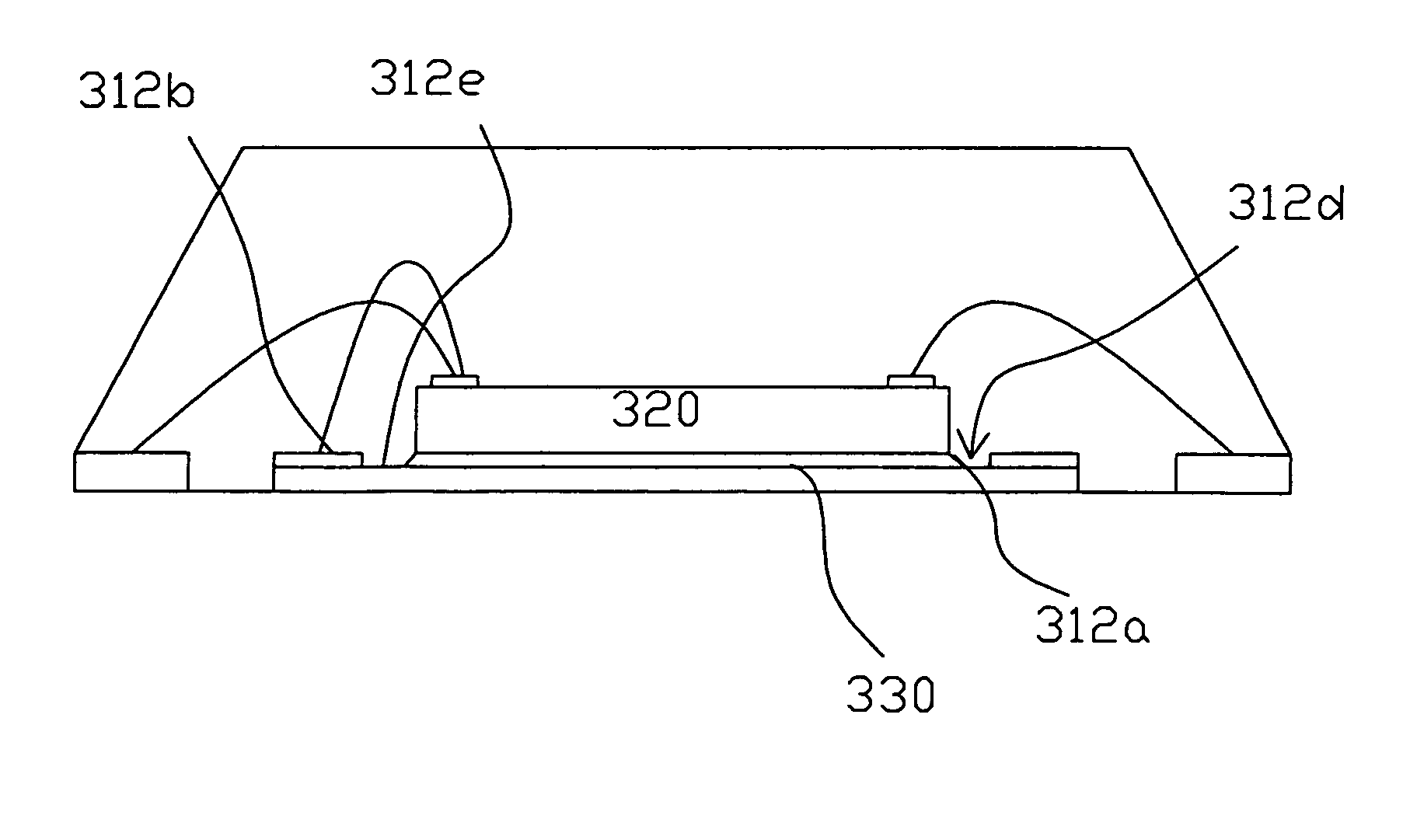
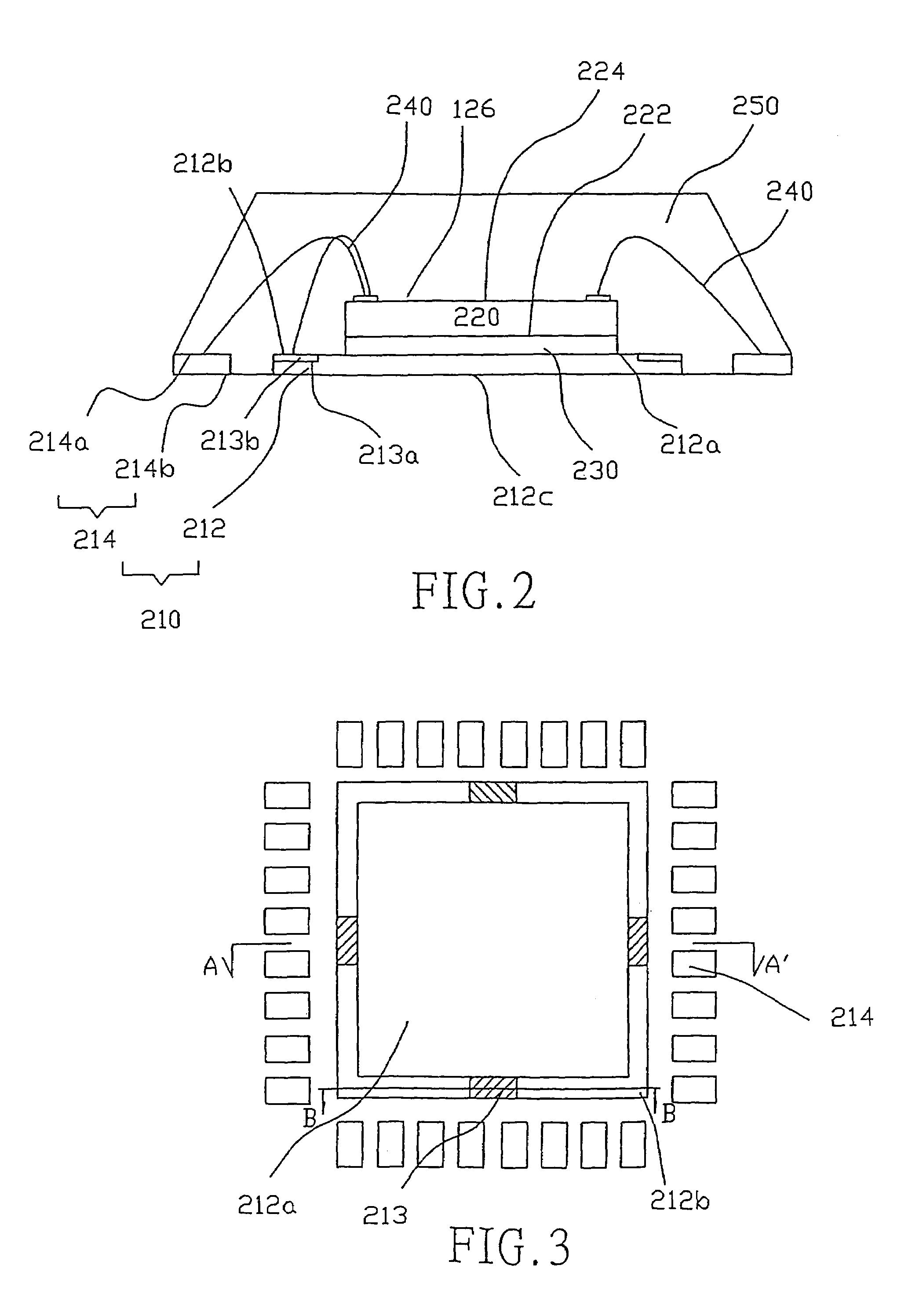
[0020]In accordance with a first preferred embodiment as shown in FIG. 2, there is provided a leadless semiconductor package. The leadless semiconductor package mainly comprises a lead frame 210, a chip 220, an adhesive 230 and a plurality of electrically conductive wires 240. Therein, the lead frame 210, such as a leadless lead-frame, has a chip paddle 212 and a plurality of leads 214 surrounding the chip paddle 212. Moreover, the chip paddle 212 has a chip disposal area 212a and a grounding area 212b surrounding the chip disposal area 212a, and the grounding area 212b at least has a recession 213. Besides, the chip 220 has a back surface 222 and an active surface 224 and the chip 220 is placed in the chip disposal area 212a of the chip paddle 212 th...


PUM


Abstract

A leadless semiconductor package mainly comprises a leadless lead-frame, a chip, a silver paste and a plurality of electrically conductive wires. The lead frame includes a chip paddle and a plurality of leads surrounding the chip paddle wherein the chip paddle has a cavity serving as a chip disposal area and a grounding area surrounding the cavity, and at least there is one recession formed on the grounding area. Besides, the chip is disposed in the cavity so that the back surface of the chip faces the chip paddle and attached onto the chip paddle via the silver paste. Moreover, the chip is electrically connected to the leads. As mentioned above, the grounding area has at least one recession formed therein, so the contact area of the leadless lead-frame with the encapsulation will be increased to enhance the attachment of the encapsulation to the leadless lead-frame.

Description

BACKGROUND OF THE INVENTION[0001]1. Field of Invention[0002]This invention relates to a leadless semiconductor package. More particularly, the present invention is related to a leadless semiconductor package with high reliability of the attachment of the encapsulation to the leadless lead-frame.[0003]2. Related Art[0004]Integrated circuits (chip) packaging technology is becoming a limiting factor for the development in packaged integrated circuits of higher performance. Semiconductor package designers are struggling to keep pace with the increase in pin count, size limitations, low profile, and other evolving requirements for packaging and mounting integrated circuits. Nowadays, ball grid array package (BGA) and chip scale package (CSP) are wildly applied to chip package with high I / Os and assembly package for thermal enhance integrated circuits.[0005]However, assembly package with lead frame possesses great marketing for that it can provide low-cost solutions for current semiconduc...

Claims


Application Information

Patent Timeline
Patent Type & Authority Patents(United States)
IPC IPC(8): H01L23/02H01L23/31H01L23/495
CPCH01L23/3107H01L24/32H01L24/49H01L23/49503H01L24/48H01L2224/32245H01L2224/48091H01L2224/48247H01L2224/48257H01L2224/49H01L2224/73265H01L2924/01029H01L2924/01047H01L2924/01079H01L2924/01082H01L2924/3011H01L2924/01033H01L2924/15747H01L2224/45144H01L2924/014H01L2924/01076H01L2924/00014H01L2924/00H01L2924/181H01L2224/05599H01L2224/85399H01L2924/14H01L24/45H01L2924/00015H01L2224/45015H01L2924/207H01L2924/00012
Inventor TSENG, CHAO-MING
Owner ADVANCED SEMICON ENG INC
Why Eureka
Try Eureka