Microfluidic device with controlled substrate conductivity

a microfluidic device and conductivity control technology, applied in the direction of positive displacement liquid engine, laboratory glassware, instruments, etc., can solve the problems of short and unpredictable life of these devices, lack of dimensional control needed for fabricating porous membranes between closely spaced microchannels, and inability to accurately and precisely modify the conductivity of small areas

Active Publication Date: 2007-03-27
CAPLIPER LIFE SCI INC
View PDF11 Cites 134 Cited by
  • Summary
  • Abstract
  • Description
  • Claims
  • Application Information

AI Technical Summary

Benefits of technology

[0014]By providing regions where substrate conductivity is increased, it is possible to run loading currents through the substrate, and thus accumulate sample components. The ion-implantation process used in embodiments of the invention can accurately and precisely modify the conductivity of small areas of an insulating substrate, so that the invention may be employed on a microfluidic device with closely packed microchannels.

Problems solved by technology

There are several problems with microfluidic devices that employ porous membranes to provide conductive paths between microchannels.
First, the lifetime of these devices is short and unpredictable due to the nature of the porous membrane.
Second, the resistance of the porous membranes may change with time.
Third, the process for fabricating porous membranes lacks the dimensional control needed to fabricate porous membranes between closely spaced microchannels.
Fourth, the nature of the conductivity of the porous membrane is not certain, and that could lead to unexpected fluctuations of conductivity both between and within microfluidic devices.
Finally, having a conductive path between microchannels may prevent the manufacture of devices with densely packed microchannels.

Method used


Image

  • Microfluidic device with controlled substrate conductivity
  • Microfluidic device with controlled substrate conductivity
  • Microfluidic device with controlled substrate conductivity

Examples


Embodiment Construction

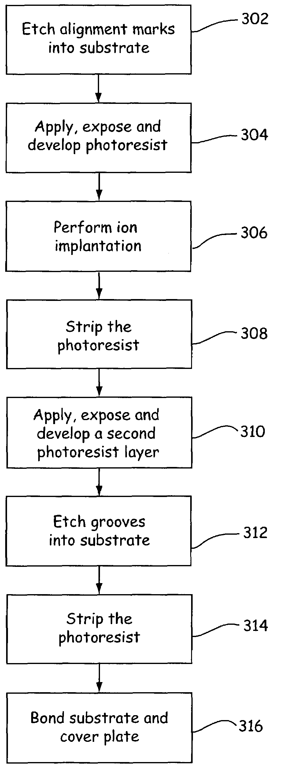
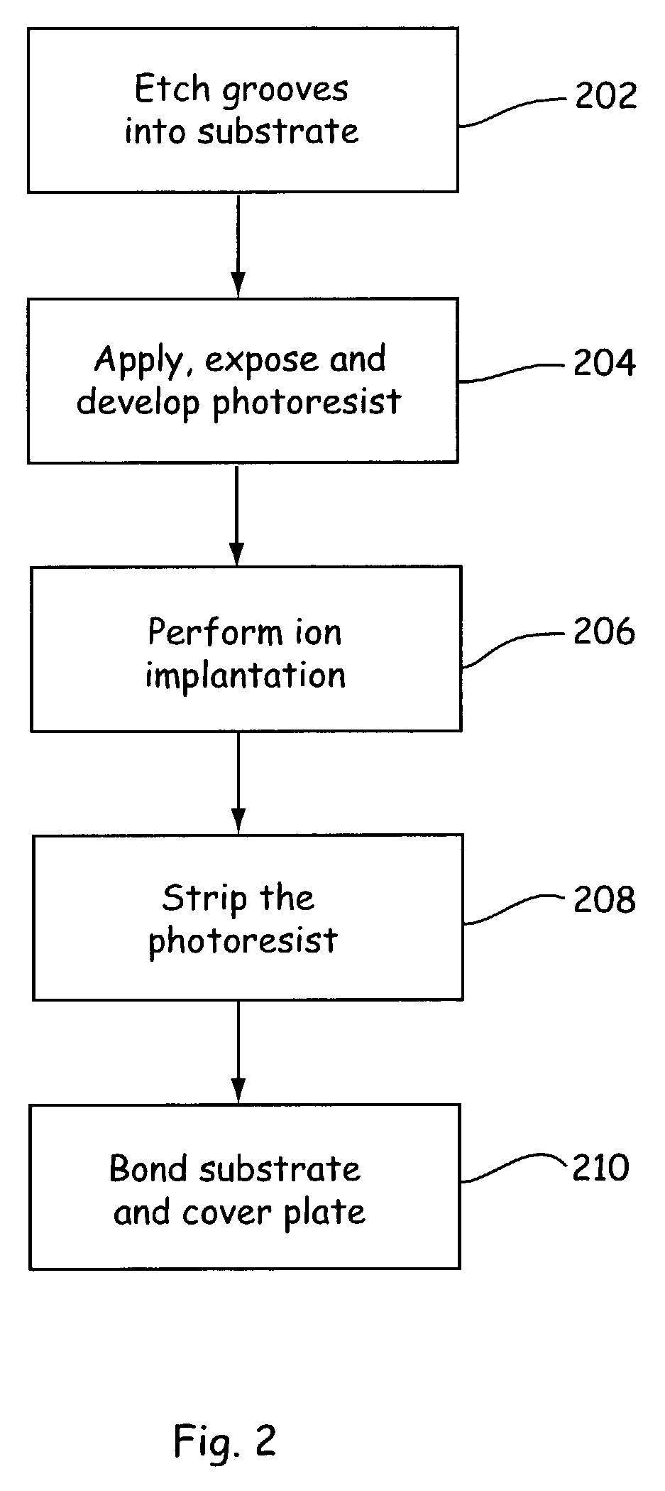
[0021]Embodiments of the present invention will now be discussed in detail. While specific features, configurations and arrangements are discussed, it should be understood that this is done for illustration purposes only. A person skilled in the relevant art will recognize that other steps, configurations and arrangements may be used without departing from the spirit and scope of the invention. It should be appreciated that the microfluidic devices in accordance with the present invention can be used to perform a variety of experiments and operations, and thus the techniques described herein could be used in connection with devices for such other functions.

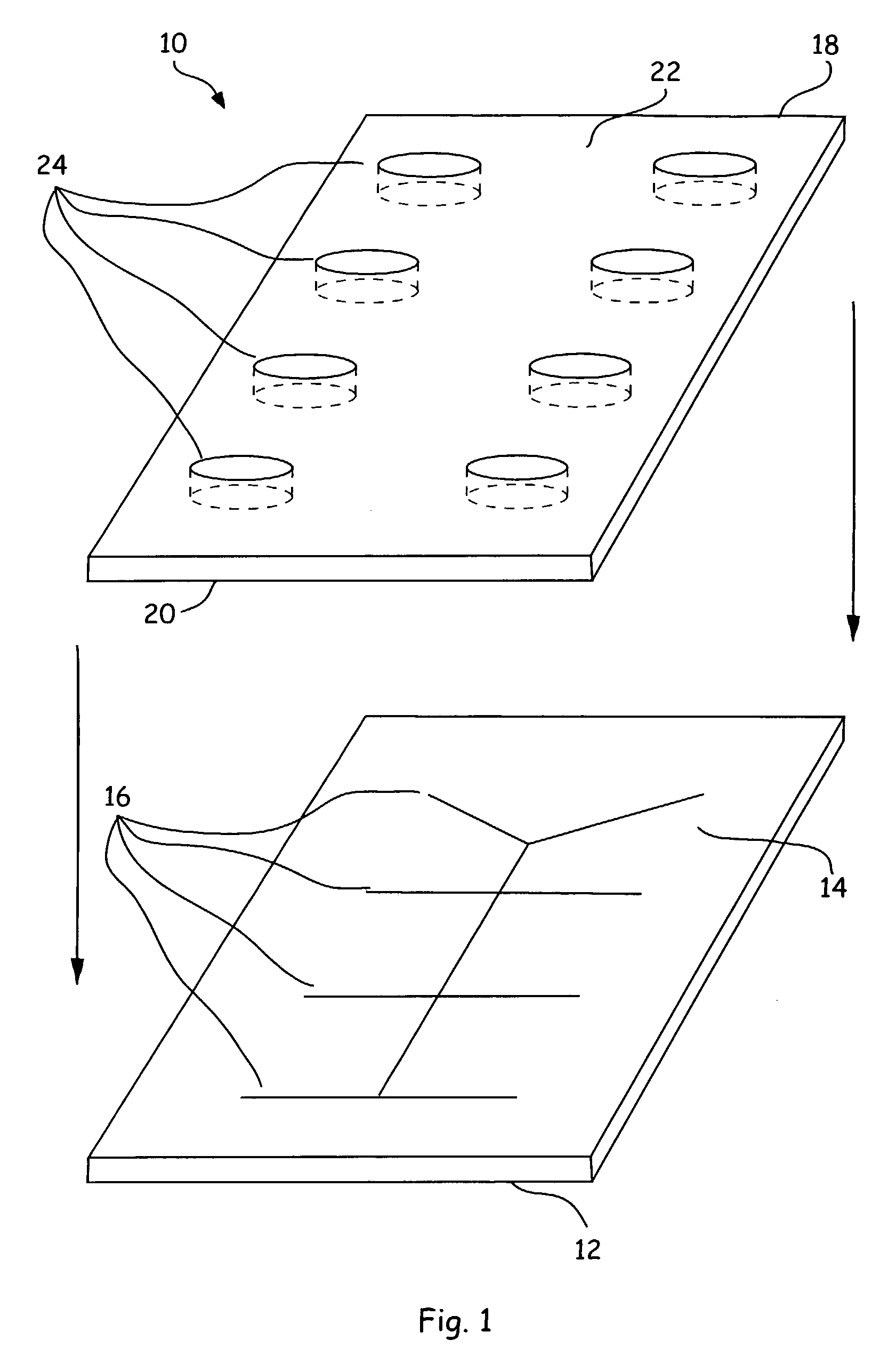
[0022]An exploded view of a microfluidic device in accordance with the invention is shown in FIG. 1. The microfluidic device 10 comprises two layers: a substrate 12 and a cover plate 18. The substrate 12 may be made of a variety of materials, including quartz, glass, polymer, ceramic or even semiconductor materials. The substrate ...


PUM

PropertyMeasurementUnit
sizeaaaaaaaaaa
physical separation distanceaaaaaaaaaa

Abstract

A method to achieve controlled conductivity in microfluidic devices, and a device formed thereby. The method comprises forming a microchannel or a well in an insulating material, and ion implanting at least one region of the insulating material at or adjacent the microchannel or well to increase conductivity of the region.

Description

CROSS REFERENCE TO RELATED APPLICATIONS[0001]This application claims the benefit of U.S. Provisional Patent Application No. 60 / 362,340, filed Mar. 8, 2002, which is incorporated herein by reference in its entirety for all purposes.BACKGROUND OF THE INVENTION[0002]1. Field of the Invention[0003]The present invention is related to microfluidic devices, and specifically to methods for modifying the conductivity of materials used in the fabrication of those devices.[0004]2. Related Art[0005]Microfluidic technology enables the miniaturization and automation of many laboratory processes. Devices employing microfluidic technology can integrate the power of an entire laboratory full of equipment and people into a single “lab-on-a-chip.” Each microfluidic device (hereafter also referred to as a “chip”) contains a network of microscopic channels, or microchannels, through which fluids can be moved and in which experiments can be performed. The design of microfluidic devices for biochemical ap...

Claims


Application Information

Patent Timeline
Patent Type & Authority Patents(United States)
IPC IPC(8): H01L21/331B01L3/02B32B5/02H01L21/00H01L21/04
CPCB01L3/502707B81B7/0006B81C1/00698G01N27/44743Y10T436/11B01L2300/0645B01L2400/0415B81B2201/058B81B2203/0338B81C2201/019G01N27/44791Y10T29/49Y10T436/2575Y10T29/41Y10T29/49002B01L2200/12
Inventor BOUSSE, LUC J.STERN, SETH R.MCREYNOLDS, RICHARD J.
Owner CAPLIPER LIFE SCI INC
Why Eureka
Try Eureka