Semiconductor storage device

a technology of semiconductors and storage devices, applied in the direction of information storage, static storage, digital storage, etc., can solve the problems of increasing the load on the external system controller, reducing the performance, and reducing the performance, so as to achieve the effect of reducing the performan

Inactive Publication Date: 2007-04-10
RENESAS ELECTRONICS CORP
View PDF1 Cites 66 Cited by
  • Summary
  • Abstract
  • Description
  • Claims
  • Application Information

AI Technical Summary

Benefits of technology

[0011]Further, the arrangement in which read / write access is always made to wait until refresh ends also invites a decline in the performance such as an access time, operating cycle and the like, and increases the load upon the external system controller.
[0019]In accordance with the present invention, an entered read / write access request is executed immediately if a refresh operation is in progress at the time of a transition from the standby state to the active state. As a result, access is implemented at high speed.
[0020]Further, in accordance with the present invention, if read / write access and a refresh request occur concurrently, refresh is postponed until later and performed in parallel with an interval in which data, which has been read out a memory cell by read access, is output. In addition, refresh is hidden externally and special refresh-control handshake with a CPU or controller that controls the semiconductor storage device is made unnecessary. As a result, access is implemented at high speed.

Problems solved by technology

This invites a decline in the performance such as an access time, operating cycle and the like.
Further, the arrangement in which read / write access is always made to wait until refresh ends also invites a decline in the performance such as an access time, operating cycle and the like, and increases the load upon the external system controller.

Method used


Image

  • Semiconductor storage device
  • Semiconductor storage device
  • Semiconductor storage device

Examples


Embodiment Construction

[0030]Preferred embodiments of the present invention will be described below.

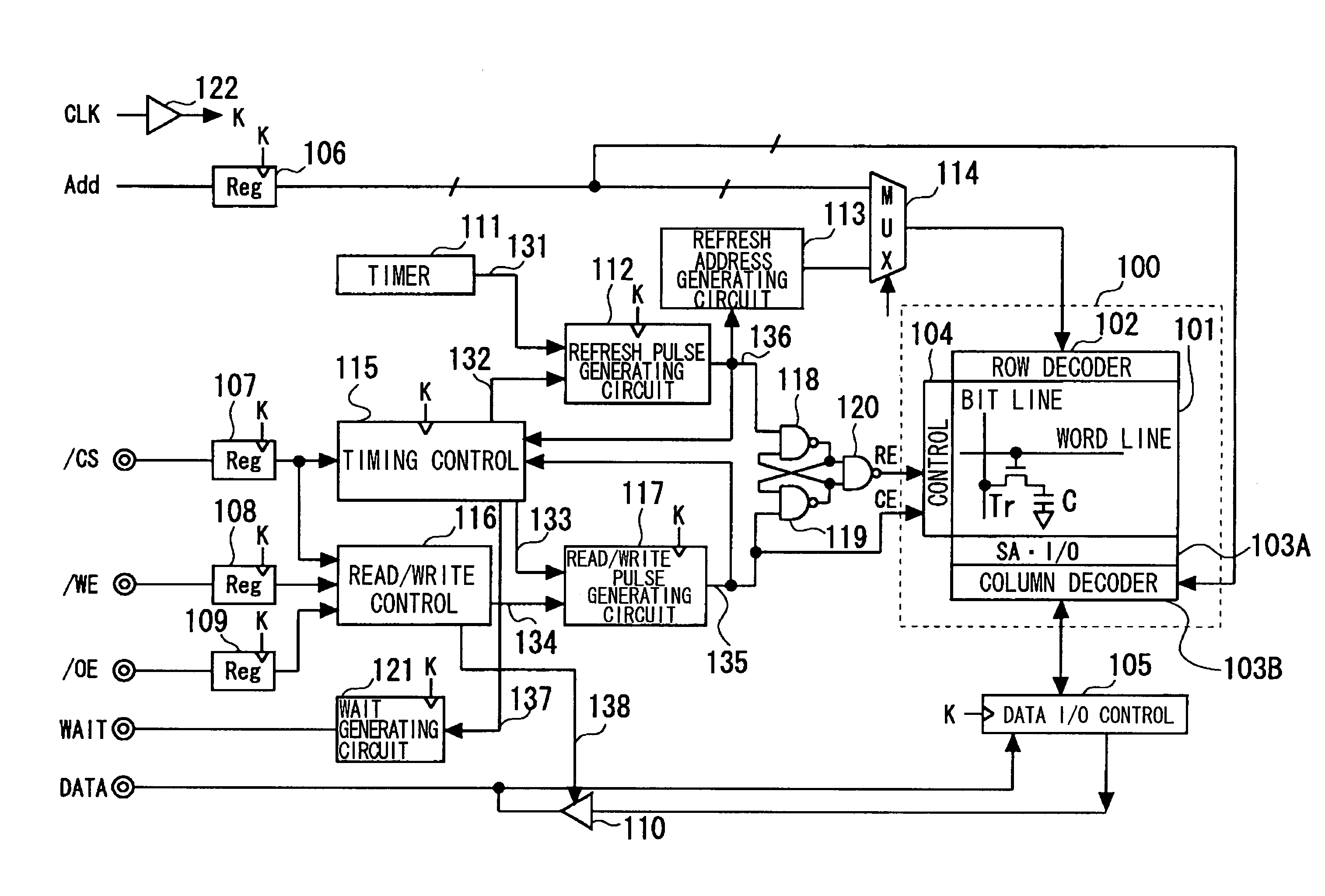
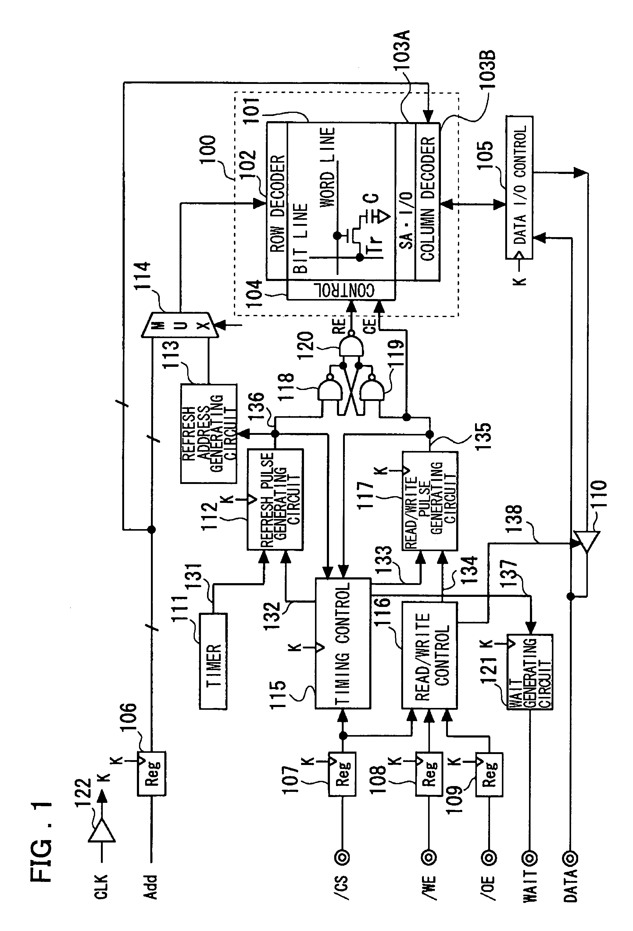
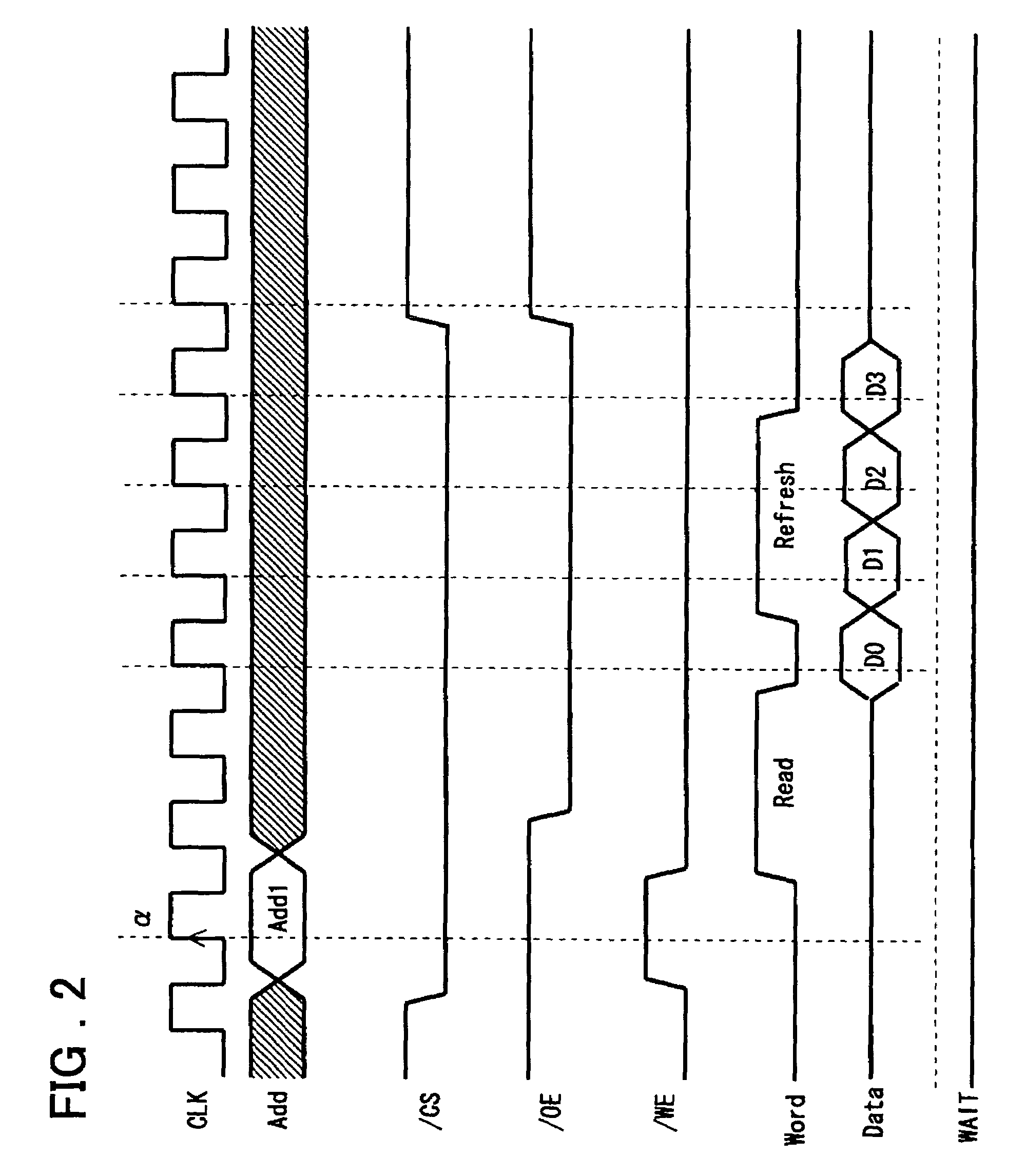
[0031]The present invention provides a semiconductor storage device in which a cell array is constituted by DRAM cells and the device is set to a standby state and an active state based upon a control signal ( / CS). Control is exercised in such a manner that when a refresh request is generated within the semiconductor storage device in concurrence with, e.g., a read operation when the semiconductor storage device is in the active state, a word line of a refresh address is activated and refresh performed in parallel with an operation for activating a word line selected by a read access request and reading out, in a burst from a data terminal (DATA), a plurality of items of data that have been read out of the cell array. In accordance with the present invention, a decline in access speed ascribable to refresh is avoided, refresh is hidden with respect to an external CPU or controller, special refresh-control h...


PUM


Abstract

Disclosed is a semiconductor storage device in which control is performed in such a manner that if the refresh operation is not being performed when a chip-select signal undergoes a transition from an inactive (standby) state to an active state, read or write access is executed immediately and if the refresh operation is in progress when the chip-select signal undergoes a transition from the inactive state to the active state, a wait signal for causing read or write access to wait is generated by a wait generating circuit.

Description

FIELD OF THE INVENTION[0001]This invention relates to a semiconductor storage device. More particularly, the invention relates to a semiconductor storage device that avoids a decline in access speed due to refresh of a semiconductor storage device having a memory cell that requires refresh in retention of data.BACKGROUND OF THE INVENTION[0002]A semiconductor storage device in which a cell array is constituted by a plurality of dynamic memory cells each requiring refresh in order for data to be retained and which functions as a static random-access memory (SRAM (such a storage device is also referred to as “pseudo SRAM”) has been used. A Mobile Specified RAM Family [also referred to as an “MSRAM” (registered trademark)] also has been developed [see NEC Memory Product Information “Mobile Specified RAM” (search conducted on Dec. 7, 2003), Internet URL:[0003]<http: / / www.necel.com / memory / japanese / products / msram / info.html>]. An MSRAM (registered trademark) is functionally compatible...

Claims


Application Information

Patent Timeline
Patent Type & Authority Patents(United States)
IPC IPC(8): G11C7/00G11C11/403G11C11/406G11C11/407G11C11/409
CPCG11C11/406G11C11/40615G11C2211/4067
Inventor TAKAHASHI, HIROYUKISHIMOYAMA, TAKATOHIROTA, TAKUYA
Owner RENESAS ELECTRONICS CORP
Why Eureka
Try Eureka