
Apparatus and method for combining writes to I/O
a technology of combining apparatus and writes, applied in the field of integrated circuit and computer system design, can solve the problems of inability to run burst cycles of graphics operations, processor write-combining makes no guarantees with respect to the order in which bits are arranged, and the burst performance capability provided by write-combining may not be useful to applications
- Summary
- Abstract
- Description
- Claims
- Application Information
AI Technical Summary
Problems solved by technology
Method used
Image

Examples
Embodiment Construction
[0020]In the following description, numerous specific details such as logic implementations, sizes and names of signals and buses, types and interrelationships of system components, and logic partitioning / integration choices are set forth in order to provide a more thorough understanding. It will be appreciated, however, by one skilled in the art that the invention may be practiced without such specific details. In other instances, control structures and gate level circuits have not been shown in detail in order not to obscure the invention. Those of ordinary skill in the art, with the included descriptions, will be able to implement appropriate logic circuits without undue experimentation.
System Architecture
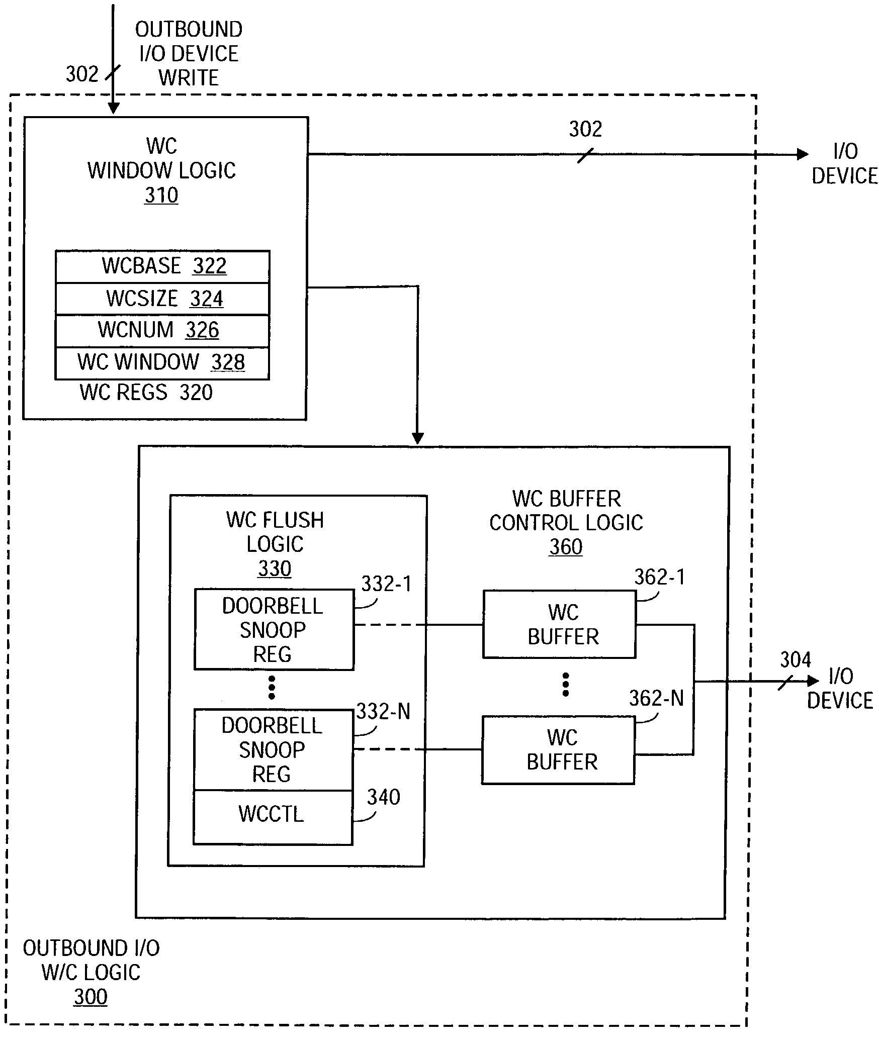
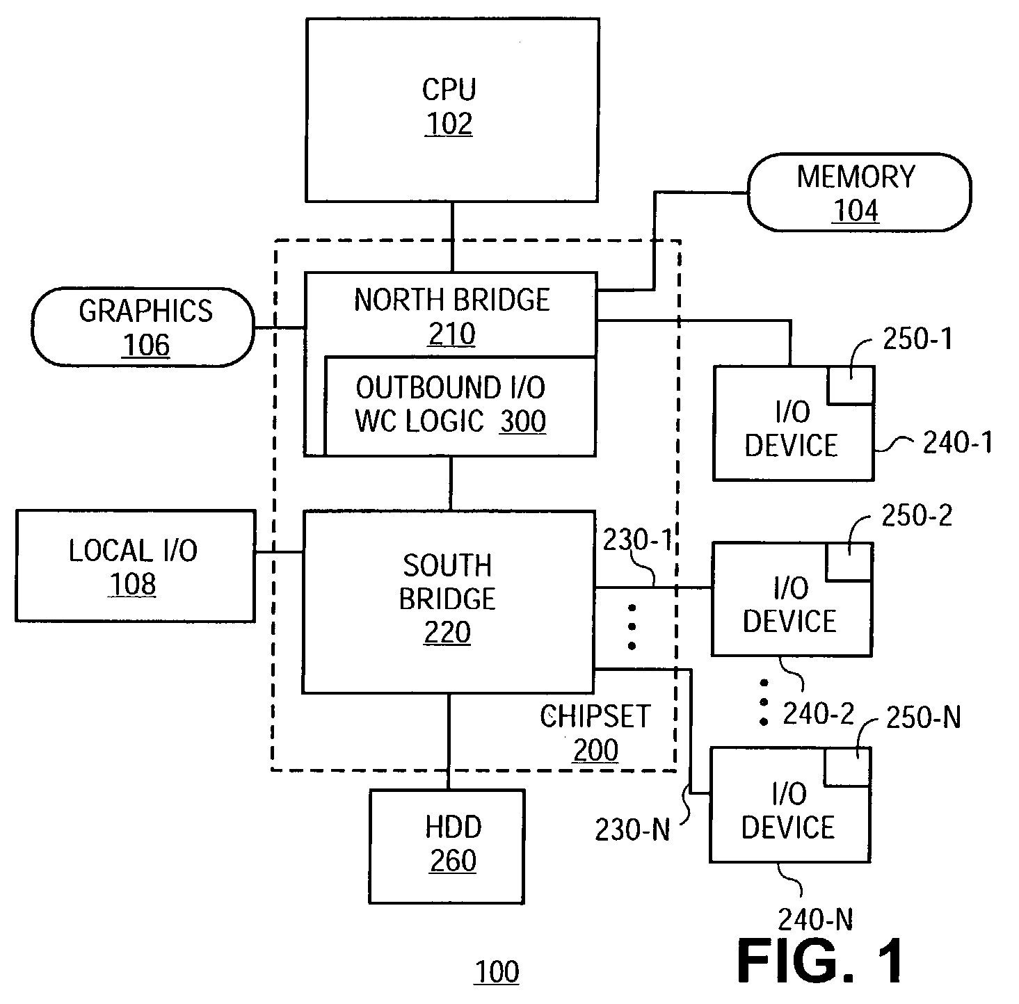
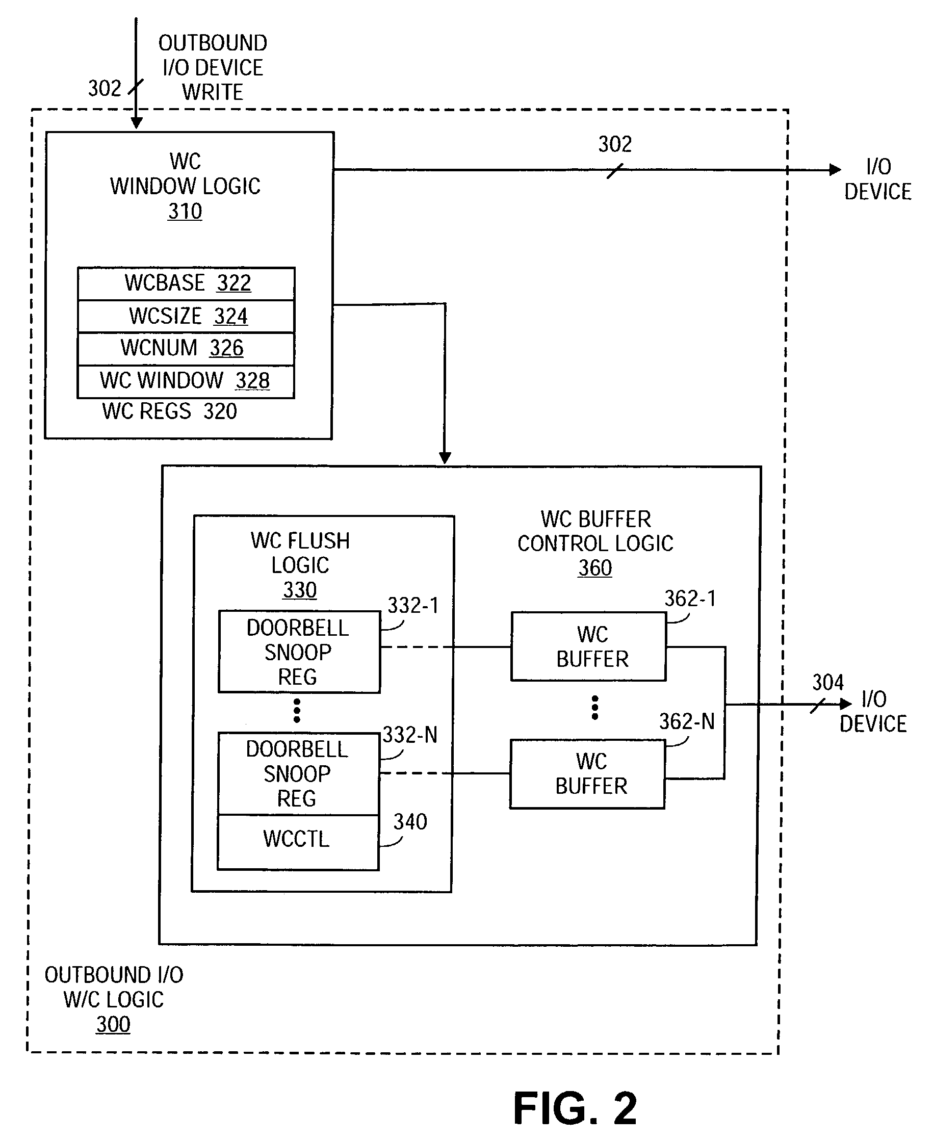
[0021]FIG. 1 is a block diagram illustrating a computer system 100, including outbound I / O (input / output) write-combining logic 300, in accordance with one embodiment of the present invention. As illustrated, computer system 100, includes a CPU 102, memory 104 and graphics contr...
PUM
 Abstract
Description
Claims
Application Information