CMOS logic gate fabricated on hybrid crystal orientations and method of forming thereof

a logic gate and hybrid crystal technology, applied in the field of semiconductor fabrication, can solve the problems of increasing the difficulty of designing system-on-a-chip implementation, increasing the difficulty of meeting esd specifications, and reducing the efficiency of esd implementation, so as to avoid the effect of harmful microloading effects

Active Publication Date: 2007-04-24
TAIWAN SEMICON MFG CO LTD
View PDF11 Cites 67 Cited by
  • Summary
  • Abstract
  • Description
  • Claims
  • Application Information

AI Technical Summary

Benefits of technology

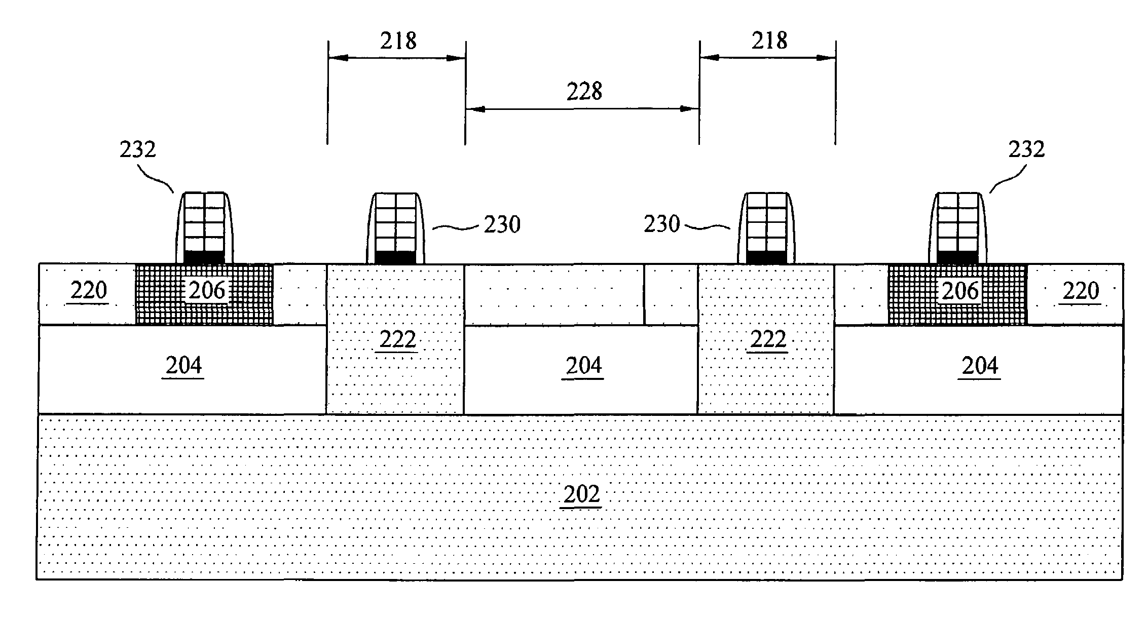
[0023]In another preferred embodiment, harmful microloading effects are avoided by limiting the active area ratio of largest N-FET region to smallest N-FET region is less than 105.

Problems solved by technology

Accordingly, one problem with the prior art is that the mobility of both electrons and holes is not optimized.
This larger device footprint generally increases the difficulty of designing system-on-a-chip implementations, which may require a large number of devices on a single chip.
Another problem in the prior art caused by using both P-FETs and N-FETs in a SOI substrate with single crystal orientation generally is potentially severe floating body effect, and the resulting history effect.
Moreover, it may increase the difficulty in meeting ESD specifications.
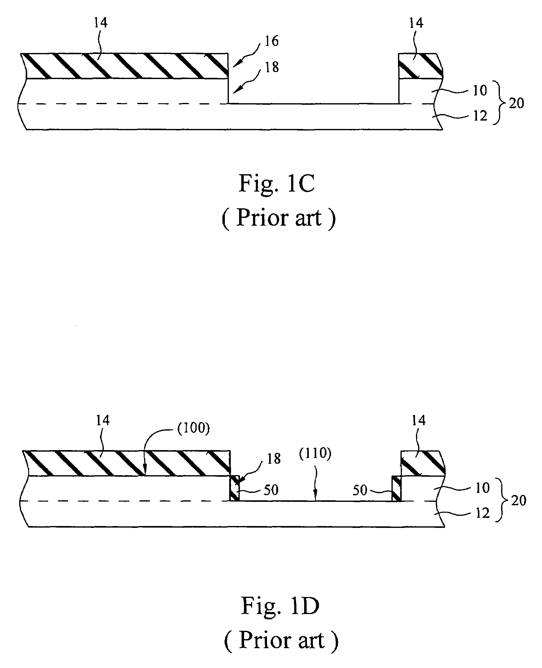
One significant problem commonly encountered in achieving this is the so-called micro-loading effect.
The micro-loading effect is also a known problem in chemical mechanical polishing (CMP) used for planarization of wafers.
Areas of the wafer that are locally sparse or dense create non-uniformity in the etching / polishing rate.
This may cause unacceptable post polish film thickness variation including dishing.
The micro-loading problem also manifests itself when fabricating FETs on hybrid crystal orientations.
This causes wide openings to grow slower than small openings.
In order to avoid a step between regions of different crystal orientation, an additional planarization step is required, thereby adding cost and complexity to the process.

Method used


Image

  • CMOS logic gate fabricated on hybrid crystal orientations and method of forming thereof
  • CMOS logic gate fabricated on hybrid crystal orientations and method of forming thereof
  • CMOS logic gate fabricated on hybrid crystal orientations and method of forming thereof

Examples


Embodiment Construction

[0038]The making and using of the presently preferred embodiments are discussed in detail below. It should be appreciated, however, that the present invention provides many applicable inventive concepts that may be embodied in a wide variety of specific contexts. The specific embodiments discussed are merely illustrative of specific ways to make and use the invention, and do not limit the scope of the invention.

[0039]The present invention will be described with respect to preferred embodiments in a specific context, namely CMOS fabrication using SOI and hybrid substrate orientations. The invention may also be applied, however, to other semiconductor devices wherein electrical isolation of neighboring devices is a concern.

[0040]U.S. Pat. No. 6,107,125 to Jaso et al., which is hereby incorporated herein by reference, describes the formation of an SOI / bulk hybrid substrate using wafer bonding. U.S. Pat. No. 4,889,829 to Kawai, which is hereby incorporated herein by reference, describes...


PUM


Abstract

In preferred embodiments of the present invention, a method of forming CMOS devices using SOI and hybrid substrate orientations is described. In accordance with a preferred embodiment, a substrate may have multiple crystal orientations. One logic gate in the substrate may comprise at least one N-FET on one crystal orientation and at least one P-FET on another crystal orientation. Another logic gate in the substrate may comprise at least one N-FET and at least one P-FET on the same orientation. Alternative embodiments further include determining the preferred cleavage planes of the substrates and orienting the substrates relative to each other in view of their respective preferred cleavage planes. In a preferred embodiment, the cleavage planes are not parallel.

Description

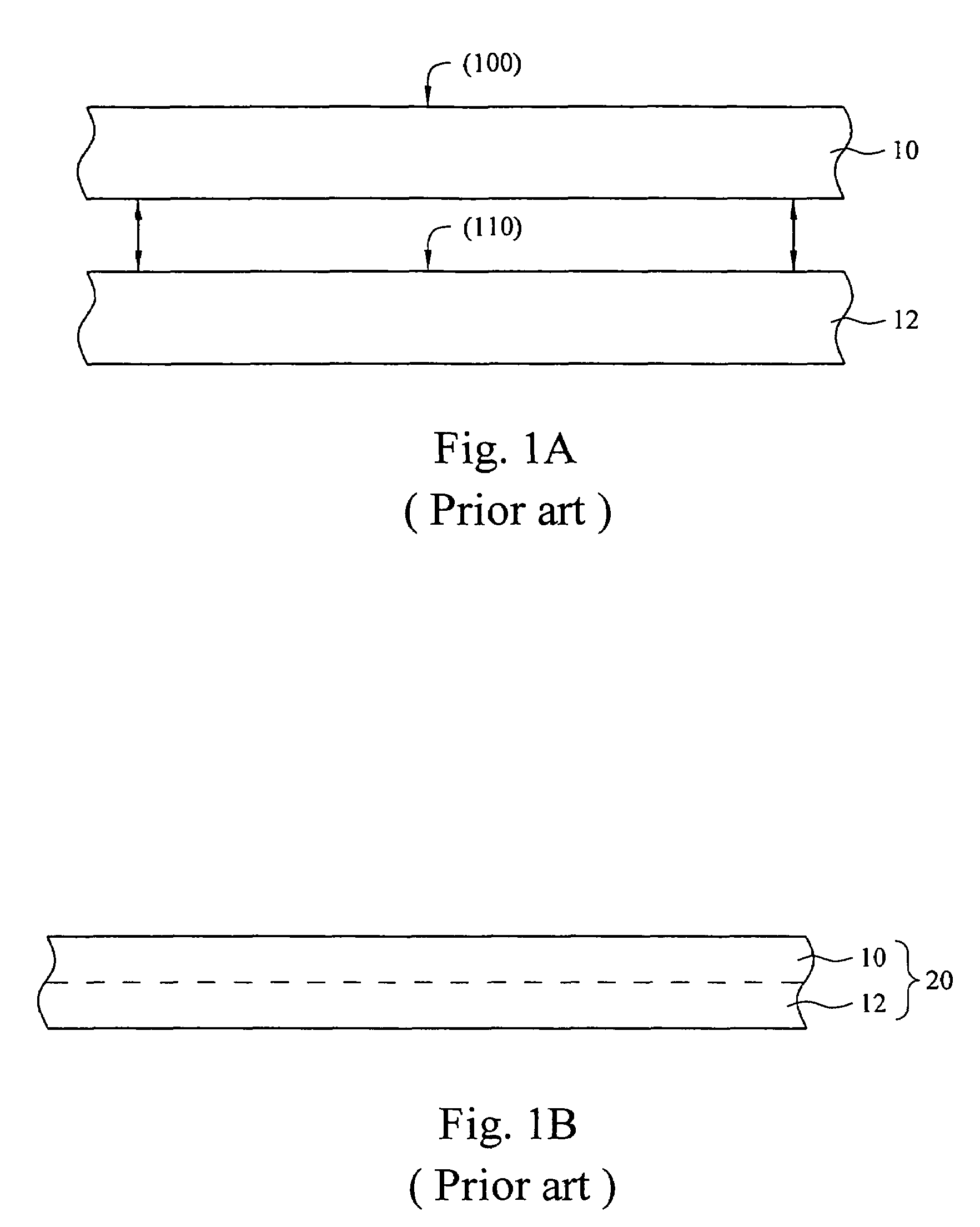
[0001]This application claims the benefit of U.S. Provisional Application No. 60 / 575,434, filed on May 28, 2004 entitled CMOS Logic Gate Fabricated on Hybrid Crystal Orientations and Method of Forming Thereof, which application is hereby incorporated herein by reference.TECHNICAL FIELD[0002]This invention relates generally to semiconductor fabrication and more particularly to a system and method for device fabrication on multiple crystal orientations.BACKGROUND[0003]In current CMOS technology, devices generally are made on one specific semiconductor substrate with a single crystal orientation. However, in silicon, electrons have their greatest mobility in the {100} family of planes, while holes have their greatest mobility in the {110} plane family. Generally, one or the other of a P-FET or an N-FET is implemented with the optimum crystal orientation, while the other functions with less than optimal carrier mobility because it is implemented with the same crystal orientation. U.S. P...

Claims


Application Information

Patent Timeline
Patent Type & Authority Patents(United States)
IPC IPC(8): H01L29/04
CPCH01L21/823807H01L21/823878H01L27/0922H01L27/1207H01L29/045H01L29/7842H01L27/1203H01L29/785
Inventor CHEN, HUNG-WEIWU, PING-KUNWANG, CHAO-HSIUNGYANG, FU-LIANGHU, CHENMING
Owner TAIWAN SEMICON MFG CO LTD
Why Eureka
Try Eureka