Expansion plane for PQFP/TQFP IR-package design

a technology of expansion plane and ir-package, which is applied in the direction of semiconductor/solid-state device details, semiconductor devices, electrical apparatus, etc., can solve the problems of adversely substantially affecting the performance of the semiconductor chip, etc., and achieve the effect of reducing electrical parasitics

Inactive Publication Date: 2007-05-08
ALTERA CORP
View PDF3 Cites 15 Cited by
  • Summary
  • Abstract
  • Description
  • Claims
  • Application Information

AI Technical Summary

Benefits of technology

[0006]To achieve the foregoing, the present invention provides a lead frame package with an expansion plane to minimize electrical parasiti...

Problems solved by technology

In particular, the performance of the semiconductor chip can be substantially affected by electrical parasitics (e.g., inductance) introduced by the intermediary...

Method used


Image

  • Expansion plane for PQFP/TQFP IR-package design
  • Expansion plane for PQFP/TQFP IR-package design
  • Expansion plane for PQFP/TQFP IR-package design

Examples


first embodiment

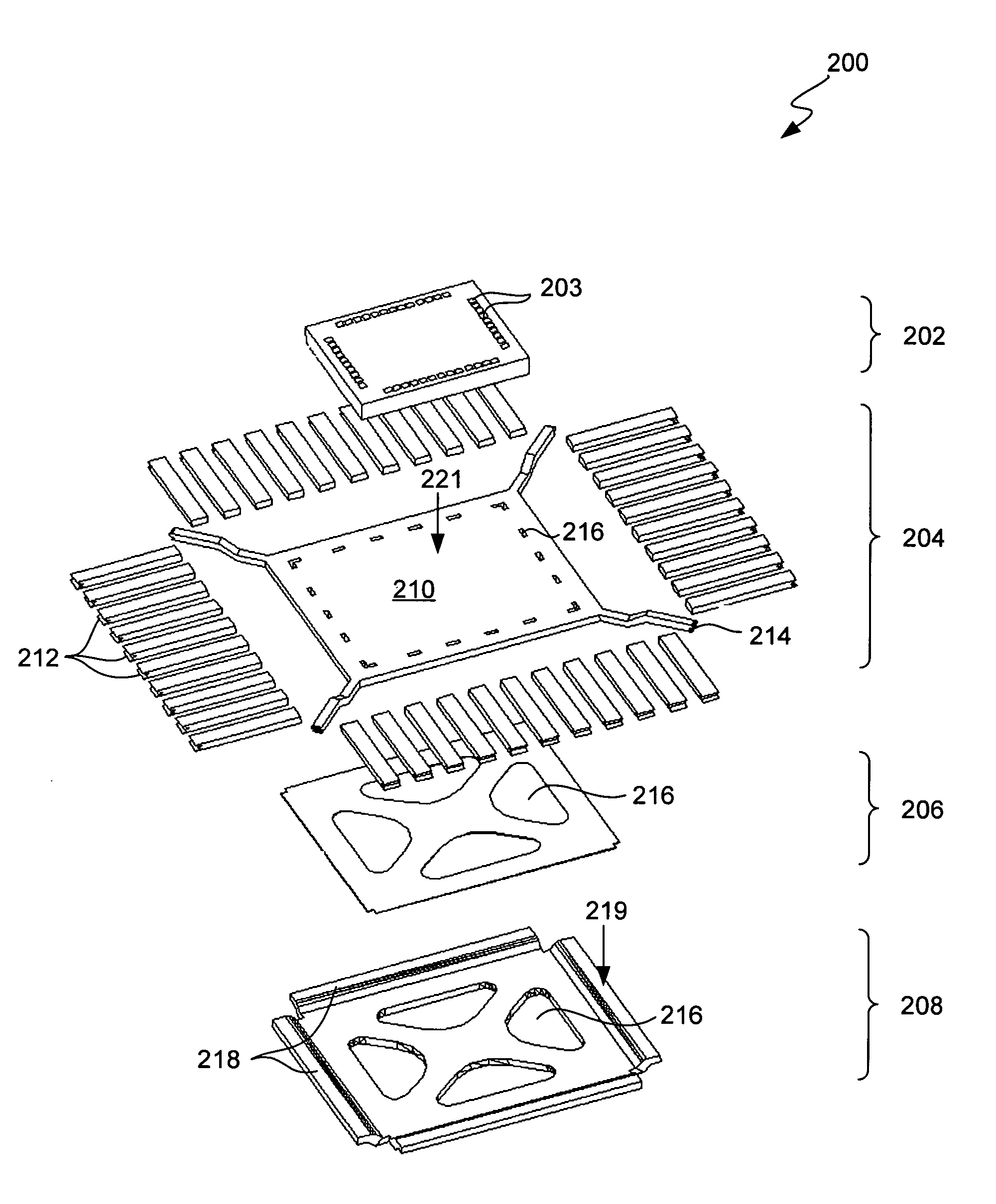
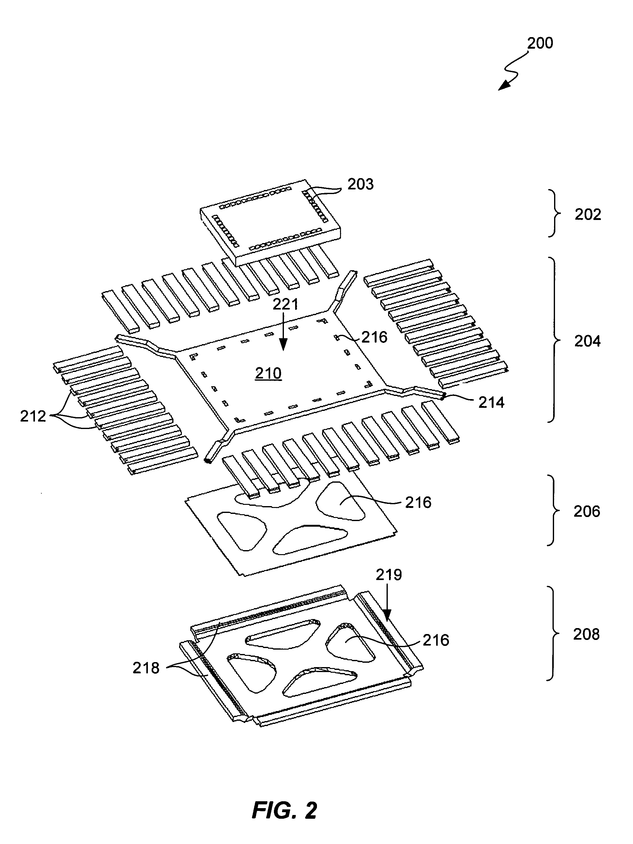
[0032]A variety of strategies are used in controlling electrical parasitics introduced by the intermediary connection. For example, FIG. 2 illustrates a perspective top view of a disassembled lead frame package 200 according to the present invention. Lead frame package 200 generally includes several components: a die 202, a package substrate 204, an insulator 206, and a bottom plate 208. All the components are configured for assembling together. For example, die 202 sits on package substrate 204, which in turn sits on insulator 206 and bottom plate 208 respectively in that order.

[0033]As shown, die 202 includes a plurality of bond pads 203 for electrically connecting to it. On the other hand, package substrate 204 includes a die attach pad 210, a plurality of tie bars 214, and a plurality of lead fingers 212. To fabricate package substrate 204, any conductive material (e.g., copper) may be used. Package substrate 204 usually has die attach pad 210 arranged such that it is surrounded...

second embodiment

[0040]Next, FIG. 4 illustrates a perspective top view of a disassembled lead frame package 400 according to the present invention. Lead frame package 400 shares similar components and processes as for lead frame package 200. Lead frame package 400 also includes several components: a die 402, a package substrate 404, an insulator 406, and a bottom plate 408. All the components are configured for assembling together. For example, die 402 sits on package substrate 404, which in turn sits on insulator 406 and bottom plate 408 respectively in that order.

[0041]As shown, die 402 includes a plurality of bond pads 403 for electrically connecting to it. On the other hand, package substrate 404 includes a die attach pad 410, a plurality of tie bars 414, and a plurality of lead fingers 412. To fabricate package substrate 404, any conductive material (e.g., copper) may be used. Package substrate 404 usually has die attach pad 410 arranged such that it is surrounded by the plurality of lead finge...

third embodiment

[0046]Finally, FIG. 6 illustrates a perspective top view of a disassembled lead frame package 600 according to the present invention. Lead frame package 600 shares similar components and processes as for lead frame package 200. Lead frame package 600 also includes several components: a die 602, a package substrate 604, an insulator 606, and a bottom plate 608. All the components are configured for assembling together. For example, die 602 sits on package substrate 604, which in turn sits on insulator 606 and bottom plate 608 respectively in that order.

[0047]As shown, die 602 includes a plurality of bond pads 603 for electrically connecting to it. On the other hand, package substrate 604 includes a die attach pad 610, a plurality of tie bars 614, and a plurality of lead fingers 612. To fabricate package substrate 604, any conductive material (e.g., copper) may be used. Package substrate 604 usually has die attach pad 610 arranged such that it is surrounded by the plurality of lead fi...


PUM


Abstract

Provided is a lead frame package with an expansion plane to minimize electrical parasitics introduced into the semiconductor chip's electrical system (e.g., power delivery system, signal loops, etc.). Also provided are methods for assembling such lead frame packages into various semiconductor packages. Generally, a lead frame package includes a down set die attach pad over an underlying bottom plate. Both the die attach pad and the bottom plate may be used as intermediary connections for either power or ground connections. As compared to conventional lead frame package having an intermediary connection, the lead frame packages of the present invention can provide for any combination of shorter wire bond lengths, more wire bond connections, improved power delivery system, or reduced amounts of electrical parasitics.

Description

BACKGROUND OF THE INVENTION[0001]This invention relates generally to semiconductor chip package assembly, and in particular to wire bonding package assembly. More specifically, the invention relates to lead frame packages with expansion planes and corresponding methods for their assembly.[0002]In order for a semiconductor chip (also referred to as a “die”) to operate, power must be supplied through a power delivery system. Some power delivery systems are configured to include an intermediary connection (e.g., power or ground) integral to the semiconductor chip package, which houses the semiconductor chip. This intermediary connection allows for the distribution of power to or from the semiconductor chip, thereby, facilitating in the operation of the semiconductor chip.[0003]A commonly used intermediary connection is an interposer ring (IR). An interposer ring is often integrated with a lead frame semiconductor package, such as a plastic quad flatpack (PQFP) or a thin quad flatpack (...

Claims


Application Information

Patent Timeline
IPC IPC(8): H01L23/495
CPCH01L23/49503H01L24/48H01L23/49589H01L24/32H01L2924/01033H01L24/45H01L2224/2919H01L2224/32245H01L2224/45144H01L2224/48091H01L2224/48227H01L2224/48237H01L2224/48247H01L2224/48465H01L2224/48599H01L2224/73265H01L2924/01029H01L2924/01077H01L2924/01079H01L2924/01082H01L2924/19041H01L2924/30107H01L2924/3011H01L2224/27013H01L2924/07802H01L2924/00014H01L2924/0665H01L2924/00H01L2924/181H01L2224/05554H01L2924/10161H01L24/49H01L2224/49171H01L2924/00012H01L2224/85399H01L2224/05599
Inventor LENG, ALLEN CHEAH CHONGCHET, TAN PING
Owner ALTERA CORP
Why Eureka
Try Eureka