
Method for manufacturing electronic component

Active Publication Date: 2007-05-29
MURATA MFG CO LTD
View PDF9 Cites 22 Cited by
  • Summary
  • Abstract
  • Description
  • Claims
  • Application Information

AI Technical Summary

Benefits of technology

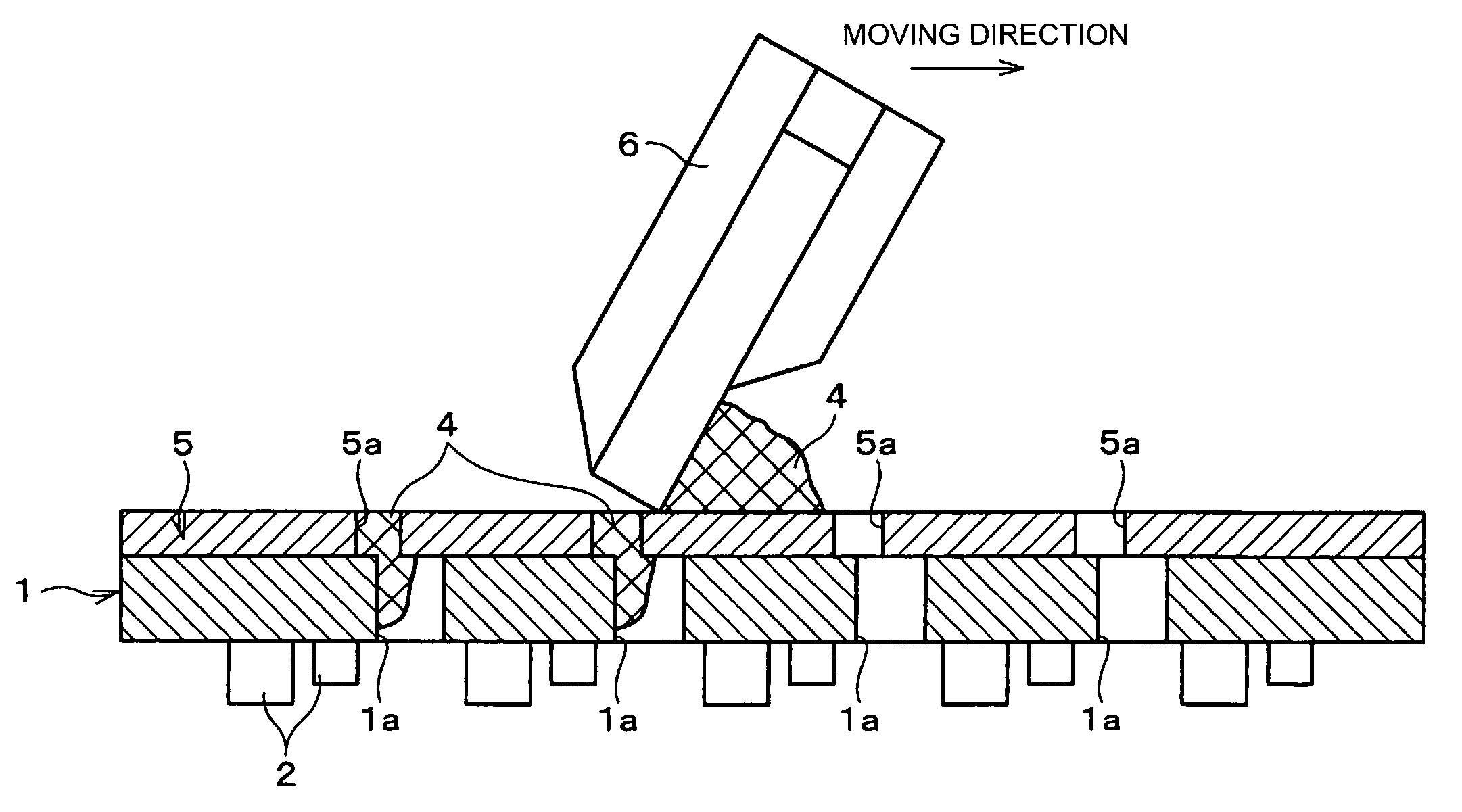
[0014]In order the solve the problems described above, preferred embodiments of the present invention provide a method for manufacturing an electronic component in which the amount of solder supplied to the through holes can be adjusted so that the metal cover can be reliably fixed to the circuit board with exactly a required amount of solder without using excessive solder, and which can thereby increase the yield of the electronic component.

Problems solved by technology

As a result, a large amount of solder cream 56 is used and costs are increased.
Therefore, malfunction due to short-circuit occurs and the yield of the electronic component is reduced.

Method used


Image

  • Method for manufacturing electronic component
  • Method for manufacturing electronic component
  • Method for manufacturing electronic component

Examples


Embodiment Construction

[0046]Preferred embodiments of the present invention will be described below with reference to FIGS. 1 to 14.

[0047]A method for manufacturing an electronic component according to a preferred embodiment of the present invention is suitable for manufacturing a module type surface-mount electronic component in which mounting elements such as IC chips, capacitors, resistors, inductors, and other electronic components and elements, are surface-mounted.

[0048]The electronic component is preferably a high-frequency composite module such as a voltage controlled oscillator (VCO), a phase-locked loop (PLL) module, a synthesizer module, a filter, a duplexer, and a radio frequency (RF) power amplifier which is used in a small communication device such as a mobile phone and which is covered with a metal cover which functions as a shield case.

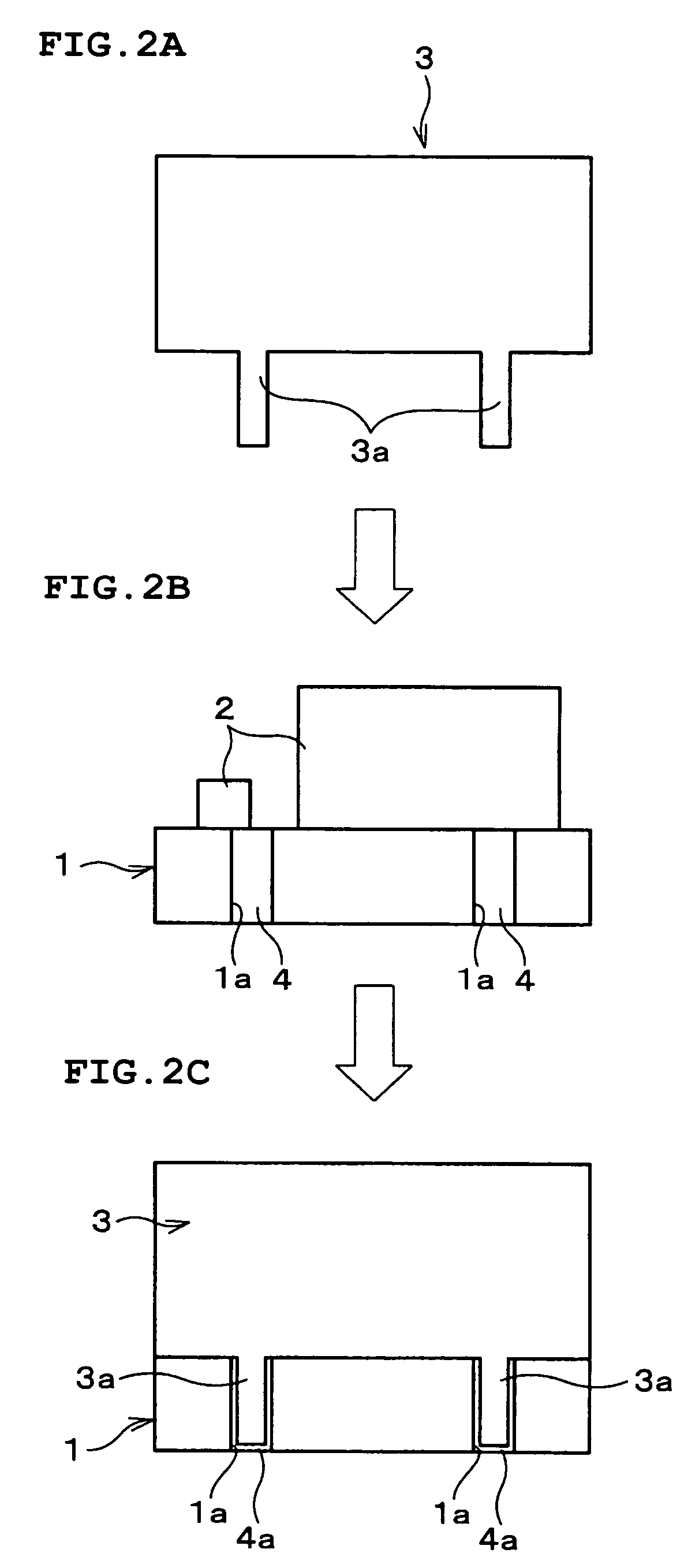
[0049]An example of an electronic component is shown in FIGS. 2A to 2C. With reference to FIG. 2B, the electronic component preferably includes a substantial...


PUM

PropertyMeasurementUnit
Shapeaaaaaaaaaa
Electrical conductoraaaaaaaaaa

Abstract

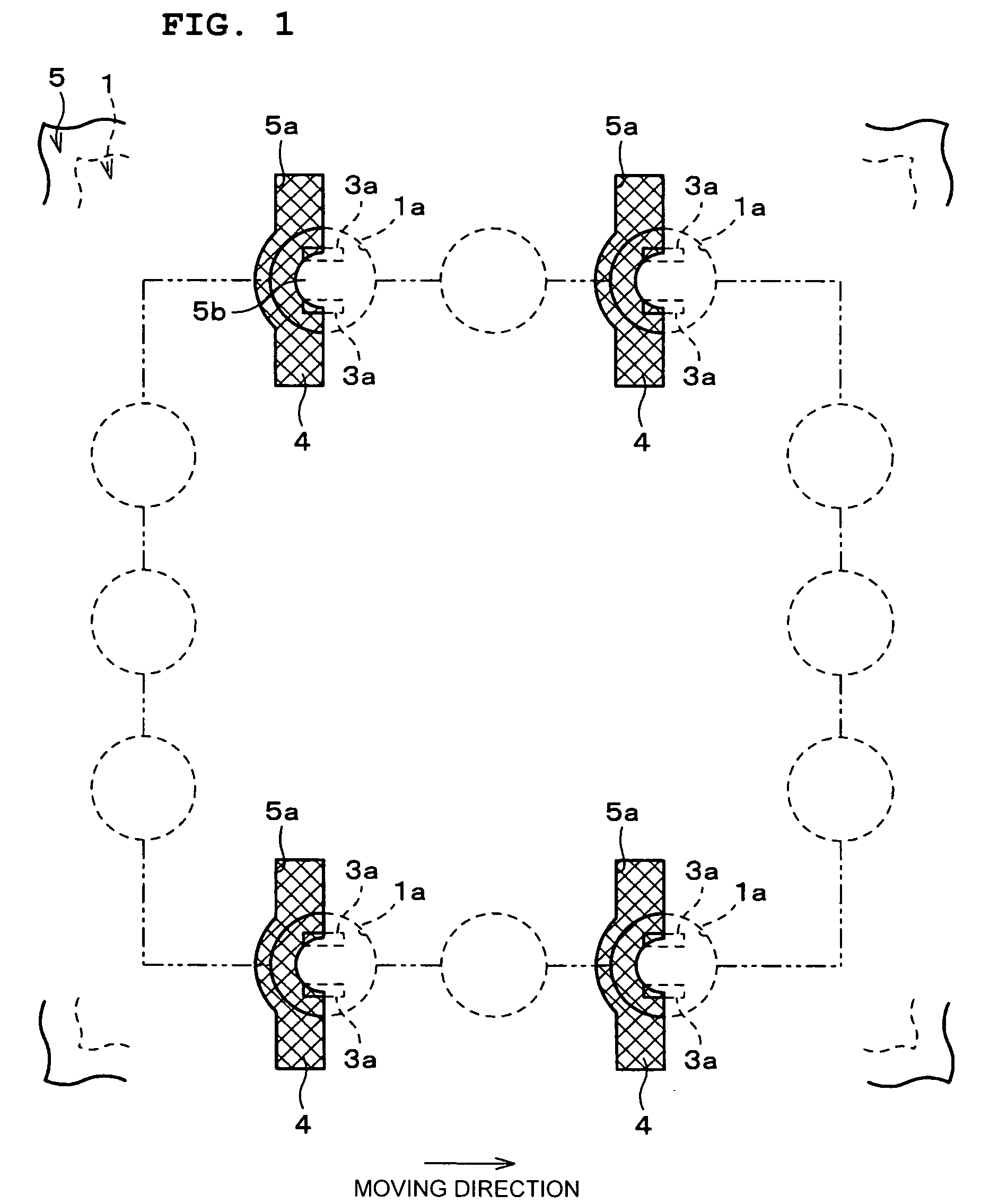
A method for manufacturing an electronic component includes the steps of inserting tabs of a cover into through holes formed in a circuit board having mounting elements on the front surface thereof, disposing a print mask having openings at positions corresponding to the through holes on the back surface of the circuit board, and supplying solder cream to the through holes through the openings by placing the solder cream on the print mask and moving the solder cream in a predetermined direction with a squeegee. The print mask is provided with projections which project upstream in the moving direction of the solder cream in openings of the print mask, and the openings are shifted upstream in the moving direction of the solder cream. In addition, the tabs are inserted into the through holes such that the width direction of the tabs is along the moving direction of the solder cream.

Description

BACKGROUND OF THE INVENTION[0001]1. Field of the Invention[0002]The present invention relates to a method for manufacturing a module type electronic component which can increase the adhesion strength of a cover attached to the electronic component and minimize variations in the adhesion strength.[0003]2. Description of the Related Art[0004]Recently, radio communication devices such as mobile phones have become popular, and module type electronic components like the one shown in FIGS. 15A to 15C have been commonly used to reduce the size, weight, and cost of the radio communication devices and to ensure their resistance to change over time and functional stability. The electronic component shown in FIGS. 15A to 15C includes a circuit board 52 on which mounting elements 50 such as IC chips, capacitors, resistances, and coils are surface-mounted and a metal cover 54 which is attached to the circuit board 52 such that the mounting elements 50 are covered with the metal cover 54.[0005]A ...

Claims


Application Information

Patent Timeline
IPC IPC(8): B29C65/00B32B37/00H05K3/00H05K3/34H01L21/48H01L21/50H01L23/04H01L23/498H05K3/12
CPCH01L21/486H01L21/50H01L23/04H01L23/49805H05K3/1225H01L21/4867Y10T29/49139H01L2924/01079H01L2924/16152H05K3/0052H05K3/3405H05K3/3447H05K3/3484H05K2201/10371H01L2924/0002Y10T29/49135Y10T29/49165H01L2924/00H05K3/3485
Inventor MURASE, TOMOHIKO
Owner MURATA MFG CO LTD
Learn More