

Connection structure of printed wiring board
a technology of connecting structure and printed wiring, which is applied in the direction of coupling contact member, printed element electric connection formation, coupling device connection, etc., can solve the problems of difficult mounting of circuit elements with high density, and achieve the effect of suitable contact performan
- Summary
- Abstract
- Description
- Claims
- Application Information
AI Technical Summary
Benefits of technology
Problems solved by technology
Method used
Image

Examples
first embodiment
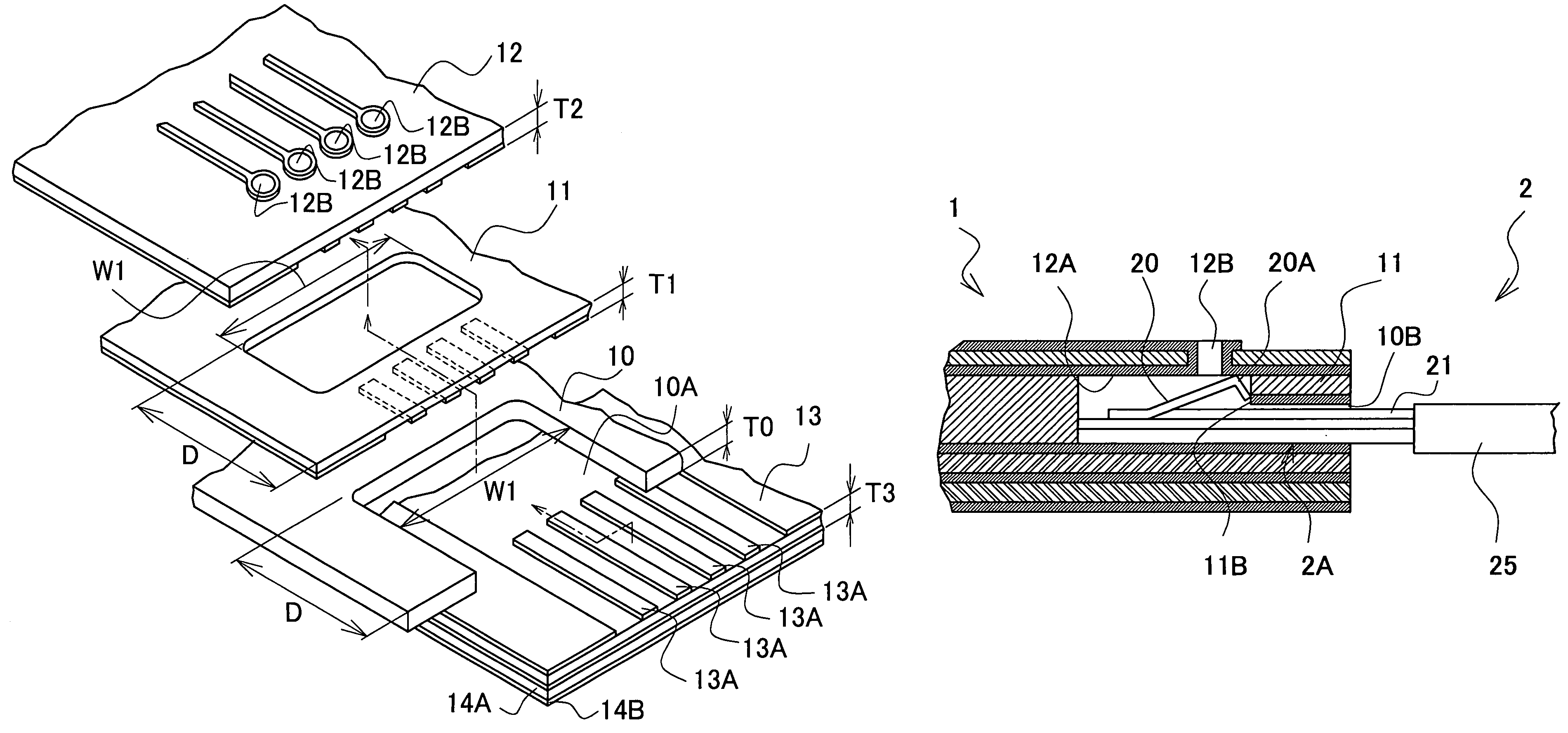
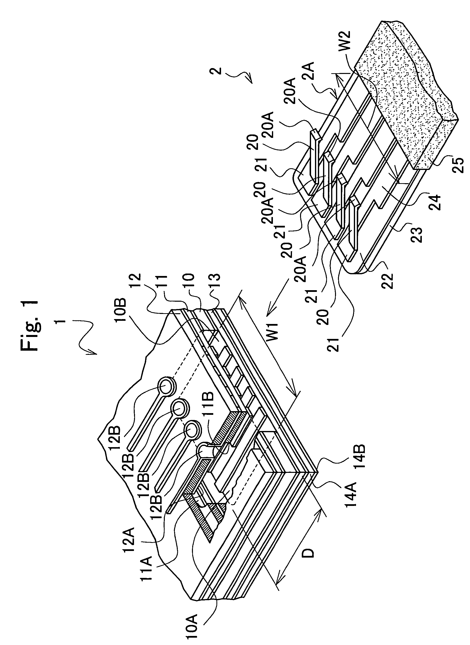
[0058]FIG. 1 is a perspective view showing a FPC 2 and a printed wiring board 1 according to a first embodiment of the present invention.
[0059]The FPC 2 includes an elongated substrate 22, a reinforcing plate 23 adhered onto the lower face of the substrate 22, and a conductor part 24 laminated on the upper face of the substrate 22.
[0060]While the FPC 2 is coated with a polyimide film 25, an end portion thereof is exposed, thereby forming an exposed conductor part 2A.
[0061]The substrate 22 has insulation properties and is formed of a thin polyimide film, for example.
[0062]The exposed conductor part 2A includes: conductors 21 which have a width of W2 and extend along the axis of the substrate 22; and elastically deformable first contact terminals 20, each of which is erected on the face of the each conductors 21 and extends toward the base end of the FPC 2.
[0063]Each first contact terminal 20 is formed by notching a part of each conductor 21 substantially in the shape of an “L”, and b...
second embodiment
[0084]In the present embodiment, a first contact terminal 40 has a different configuration from that of the first embodiment.
[0085]FIG. 5 is a perspective view of an FPC 4 according to the second embodiment of the present invention.
[0086]That is to say, each first contact terminal 40 is formed by notching a part of each conductor 21 substantially in the shape of a “C”, and by bending up the notched part. A first contact terminal 40 is formed with approximately half the width of the conductor 21. Each first contact terminal 40 has a protrusion 40A at the tip thereof, which is bent down in the direction substantially perpendicular to a conductor 21, in the same way as with the first contact terminal 20 according to the first embodiment.
third embodiment
[0087]In the present embodiment, an exposed conductor part 3A of an FPC 3 has a different configuration from that of the first embodiment.
[0088]FIG. 6 is a perspective view of the FPC 3 and the printed wiring board 1 according to the present embodiment.
[0089]The exposed conductor part 3A of the FPC 3 includes: plural conductors 31 extending along the axial direction of the substrate 22; and elastically deformable second contact terminals 30, each of which is formed on the face of each conductor 31.
[0090]Each second contact terminal 30 extends toward the base end of the FPC 3. The tip thereof is bent toward the conductors 31. That is to say, each second contact terminal 30 includes a flat portion 30A fixed to the conductors 31, a first inclined portion 30B extending upward from the flat portion 30A, a second inclined portion 30C extending downward from the first inclined portion 30B, and a third inclined portion 30D extending upward from the second inclined portion 30C.
[0091]The subs...
PUM
 Abstract
Description
Claims
Application Information