Chip-size package structure and method of the same

a chip-size and package technology, applied in the field of chip-size package structure, can solve the problems of reducing the yield, reducing the yield, and the frame package technology is already not suitable for advanced semiconductor dice, so as to reduce the contact resistance of the chip-size package structure, reduce the cost of the package structure, and raise the yield and reliability of the package structure

Active Publication Date: 2007-07-03
ADL ENERGY CORP
View PDF4 Cites 108 Cited by
  • Summary
  • Abstract
  • Description
  • Claims
  • Application Information

AI Technical Summary

Benefits of technology

[0009]Still another objective of the present invention is to reduce the contact resistance of the chip-size package structure.
[0010]Another objective of the present invention is to lower the cost of the package structure.
[0011]Still another objective of the present invention is to raise the yield and reliability of the package structure.

Problems solved by technology

It causes the packaging for the semiconductor dice to become more difficult and decrease the yield.
The earlier lead frame package technology is already not suitable for the advanced semiconductor dice due to the density of the pins thereof is too high.
Therefore, number of the pads is limited and a too short pitch among pads results in a problem of signal coupling or signal interface.
Moreover, the size of die gradually become smaller and the packaged IC of the die does not have standard size by some package technologies (such as chip size package), but test equipment, package equipment, etc. for some fixed sizes die or packages can not be kept on using.
Besides, bad performance of the inter-connection and higher contact resistance of the die and bad thermal conductor of the base will result in reduction or failure of function of the die.

Method used


Image

  • Chip-size package structure and method of the same
  • Chip-size package structure and method of the same
  • Chip-size package structure and method of the same

Examples


Embodiment Construction

[0022]Some sample embodiments of the present invention will now be described in greater detail. Nevertheless, it should be recognized that the present invention can be practiced in a wide range of other embodiments besides those explicitly described, and the scope of the present invention is expressly not limited expect as specified in the accompanying claims.

[0023]Then, the components of the different elements are not shown to scale. Some dimensions of the related components are exaggerated and meaningless portions are not drawn to provide a more clear description and comprehension of the present invention.

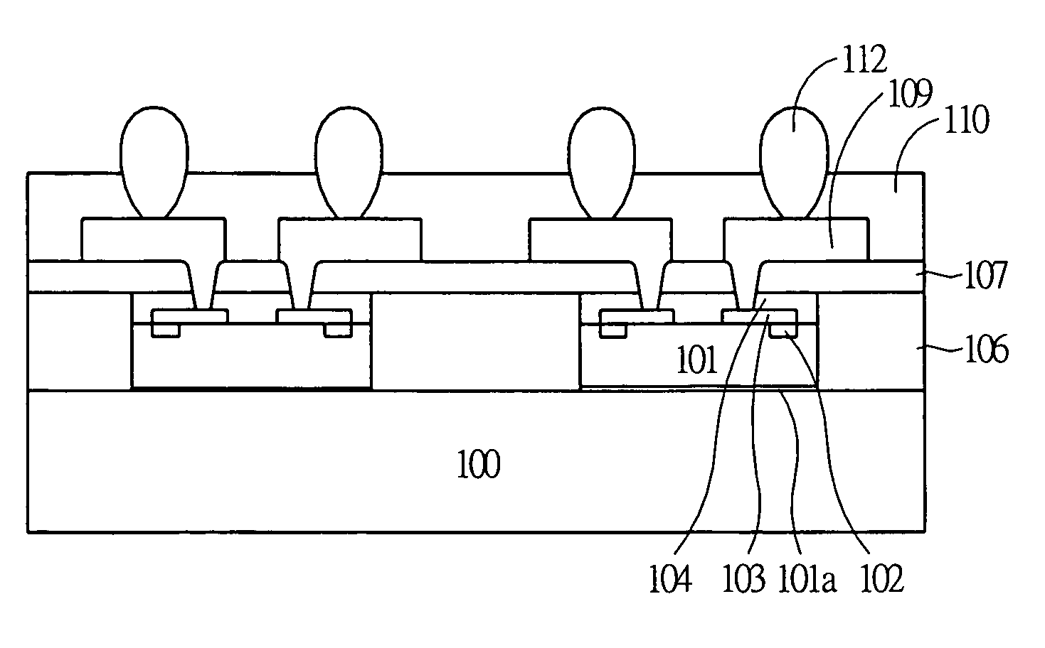
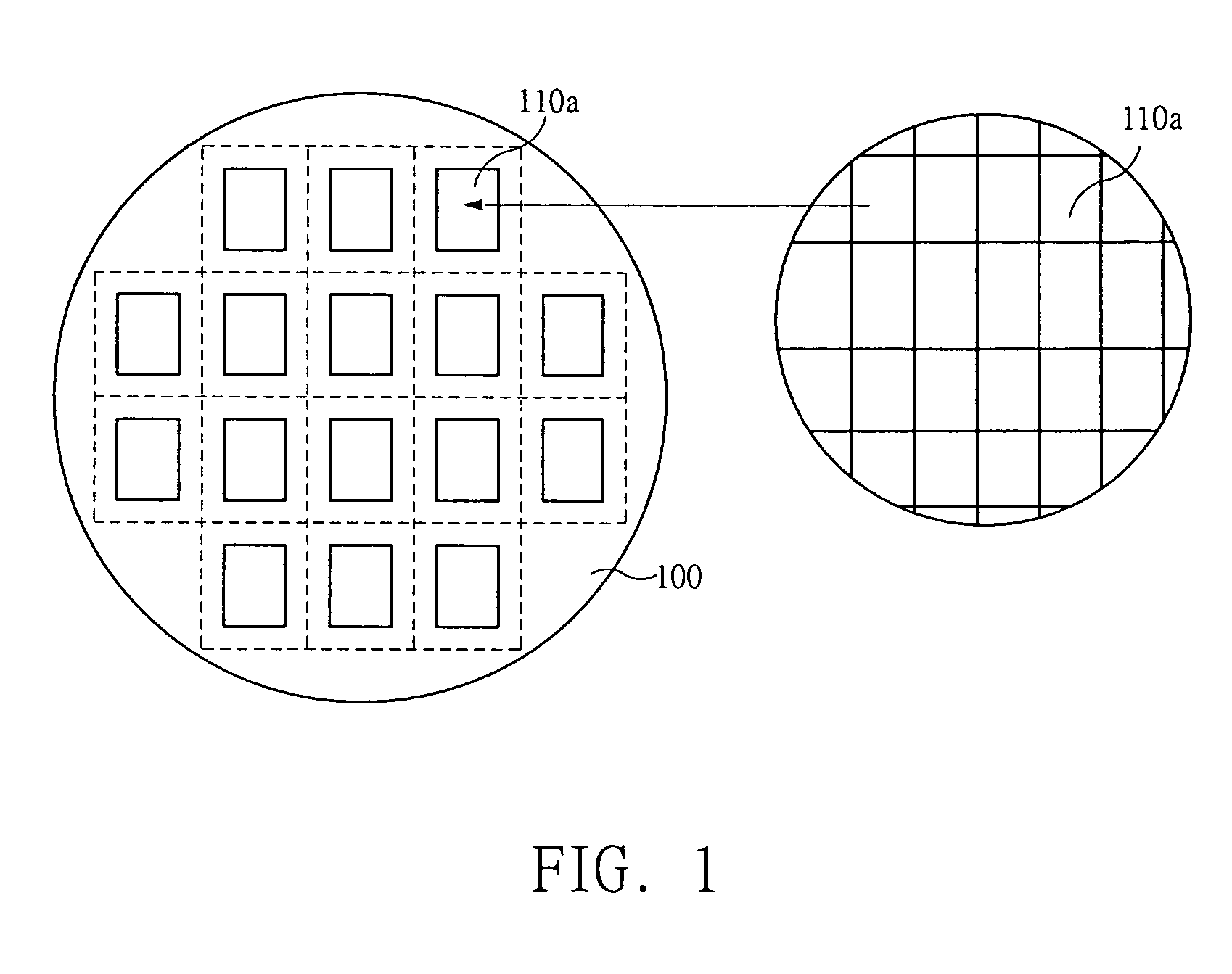
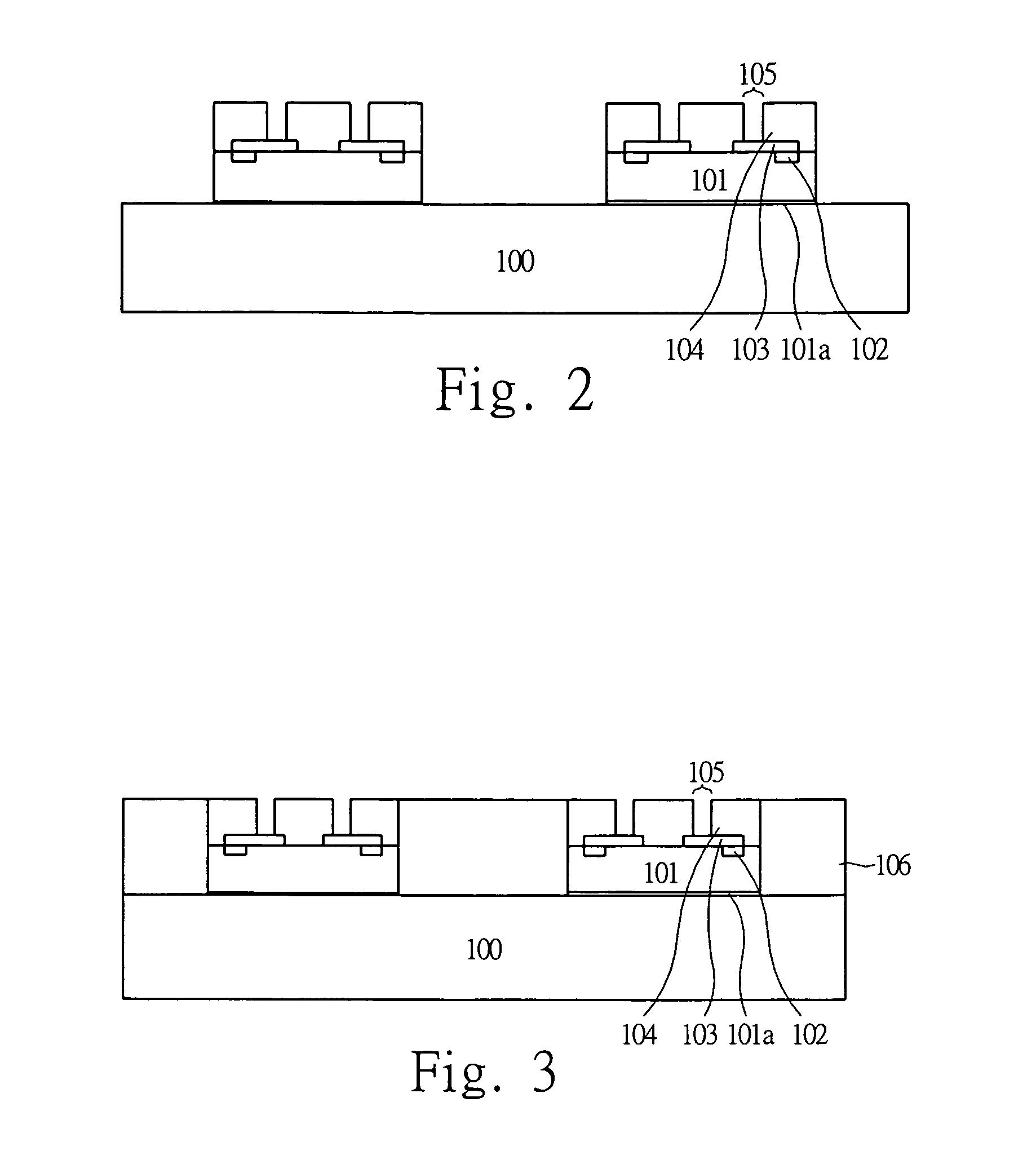
[0024]The present invention includes a step of picking and placing standard dice on an additional base for obtaining an appropriate and wider distance between dice than the original distance of dice on a wafer. Therefore, the package structure has a larger size of balls array than the size of the die to avoid the short pitch problem between balls. The method includes a step of pi...


PUM


Abstract

The method includes a step of picking and placing standard good dice on a base for obtaining an appropriate and wider distance between dice than the original distance of dice on a wafer. The method of the chip-size package comprises the steps of separating dice on a wafer and picking and placing the dice on a base and filling a first material layer on the base into a space among the dice on the base. A dielectric layer with first openings is patterned to expose a portion of a conductive line of the dice. A conductive material is filled into the first openings and on the dielectric layer. Subsequently, a second material layer is formed to have a second openings exposing the conductive material and then welding solder balls on the second openings.

Description

FIELD OF THE INVENTION[0001]This invention relates to a package for semiconductors, and more particularly to a chip-size package.BACKGROUND OF THE INVENTIONDescription of the Prior Art[0002]The semiconductor technologies are developing very fast, and especially semiconductor dice have a tendency toward miniaturization. However, the requirements for the functions of the semiconductor dice have an opposite tendency to variety. Namely, the semiconductor dice must have more I / O pads into a smaller area, so the density of the pins is raised quickly. It causes the packaging for the semiconductor dice to become more difficult and decrease the yield.[0003]The main purpose of the package structure is to protect the dice from outside damages. Furthermore, the heat generated by the dice must be diffused efficiently through the package structure to ensure the operation the dice.[0004]The earlier lead frame package technology is already not suitable for the advanced semiconductor dice due to the...

Claims


Application Information

Patent Timeline
Patent Type & Authority Patents(United States)
IPC IPC(8): H01L21/44H01L21/56H01L21/60
CPCH01L23/49816H01L23/5389H01L24/19H01L2224/04105H01L2224/20H01L2224/211H01L2924/01013H01L2924/01015H01L2924/01027H01L2924/01029H01L2924/01033H01L2924/01075H01L2924/01077H01L2924/01078H01L2924/01079H01L2924/01082H01L2924/09701H01L2924/14H01L2924/15311H01L24/97H01L2224/12105H01L2224/32225H01L2224/32245H01L2224/73267H01L2224/92244H01L2224/97H01L2924/01006H01L2924/01068H01L2224/94H01L2224/83874H01L2224/83H01L2224/82H01L2224/03H01L23/48H01L21/60
Inventor YANG, WEN KUN
Owner ADL ENERGY CORP
Why Eureka
Try Eureka