Embedding memory between tile arrangement of a configurable IC

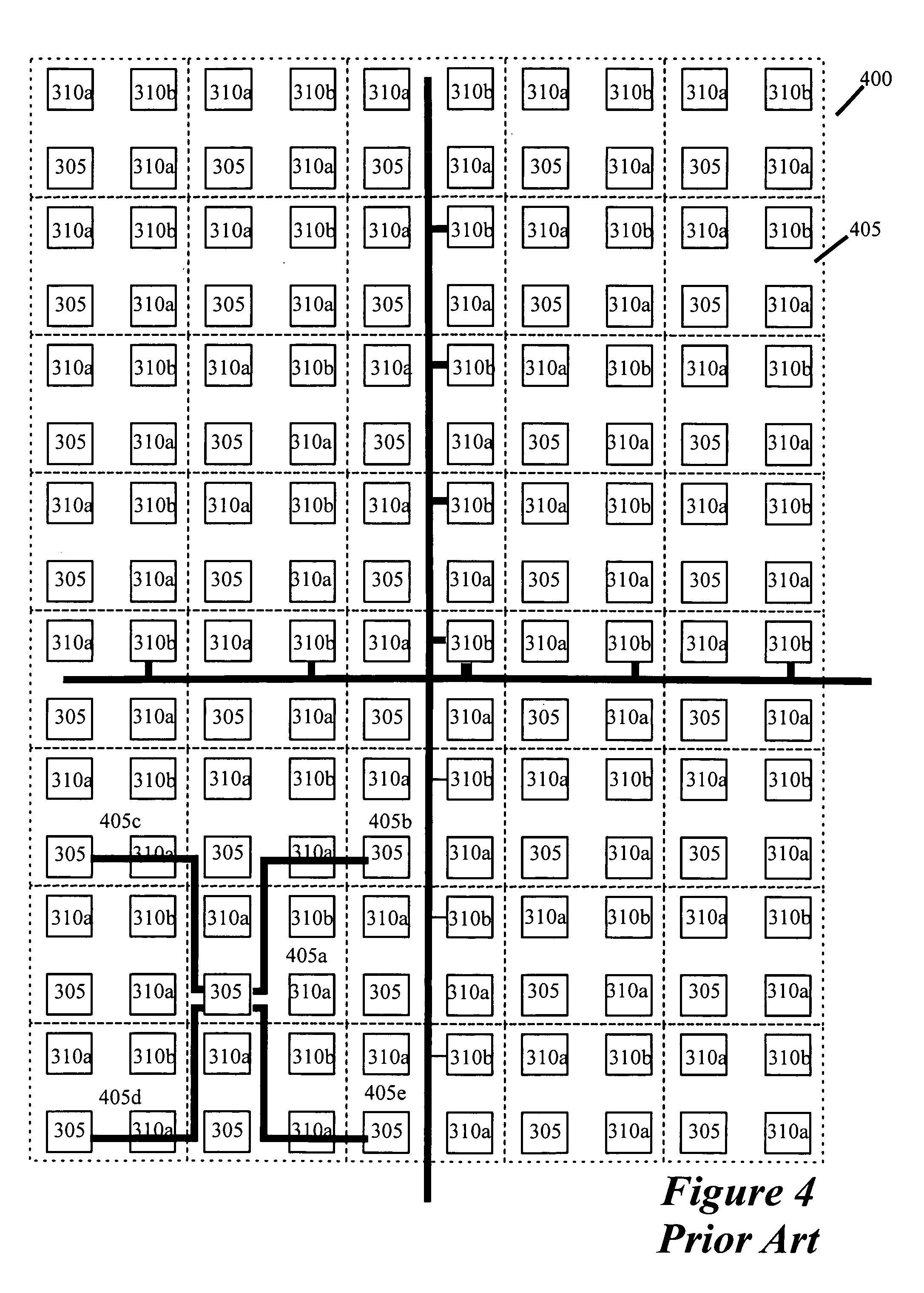
a configurable ic and memory technology, applied in the field of embedding memory between tile arrangements of configurable ics, can solve the problems of inefficient and expensive connection architecture illustrated in fig. 4, cycle undesirable, and inefficient uniform connection architecture of fig. 4

Inactive Publication Date: 2007-07-10
ALTERA CORP
View PDF114 Cites 67 Cited by
  • Summary
  • Abstract
  • Description
  • Claims
  • Application Information

AI Technical Summary

Problems solved by technology

This requirement makes the connection architecture illustrated in FIG. 4 inefficient and expensive as each connection requires the use of transistor switching logic.
Such cycles are undesirable as they come at the expense of reachability of oth

Method used


Image

  • Embedding memory between tile arrangement of a configurable IC
  • Embedding memory between tile arrangement of a configurable IC
  • Embedding memory between tile arrangement of a configurable IC

Examples


Embodiment Construction

[0071]In the following description, numerous details are set forth for purpose of explanation. However, one of ordinary skill in the art will realize that the invention may be practiced without the use of these specific details. For instance, not all embodiments of the invention need to be practiced with the specific number of bits and / or specific devices (e.g., multiplexers) referred to below. In other instances, well-known structures and devices are shown in block diagram form in order not to obscure the description of the invention with unnecessary detail.

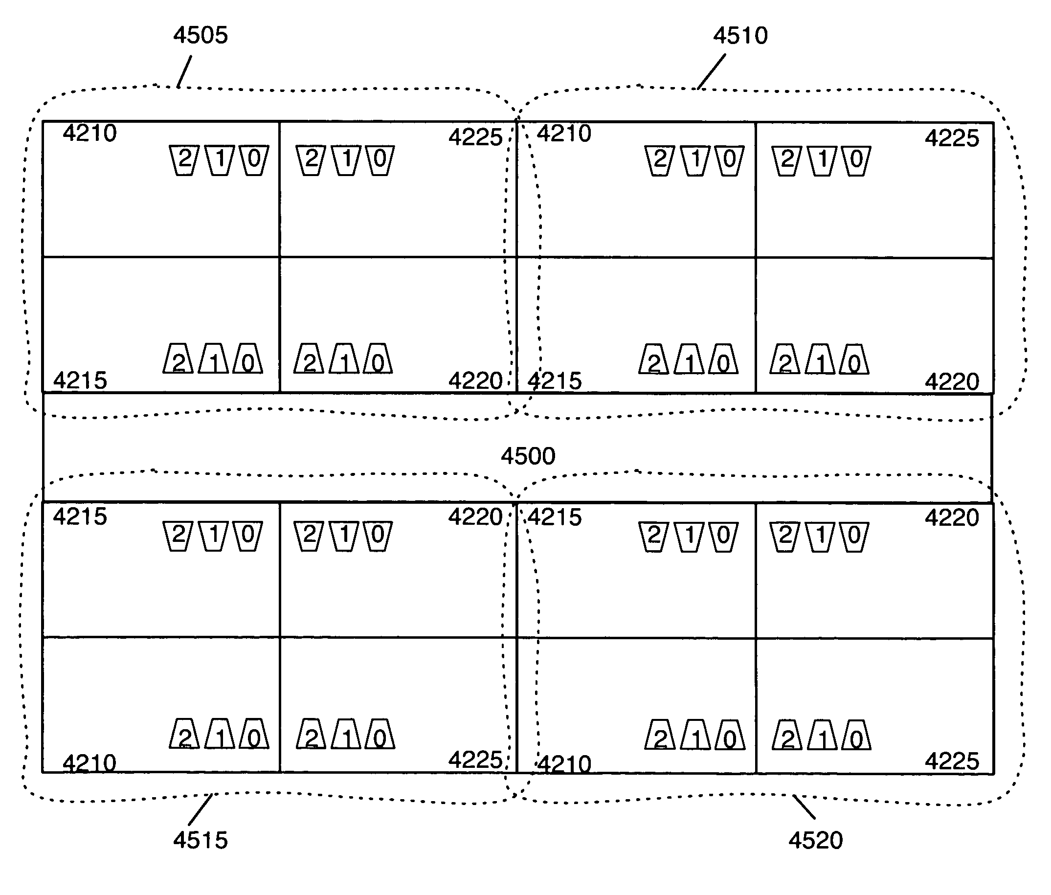
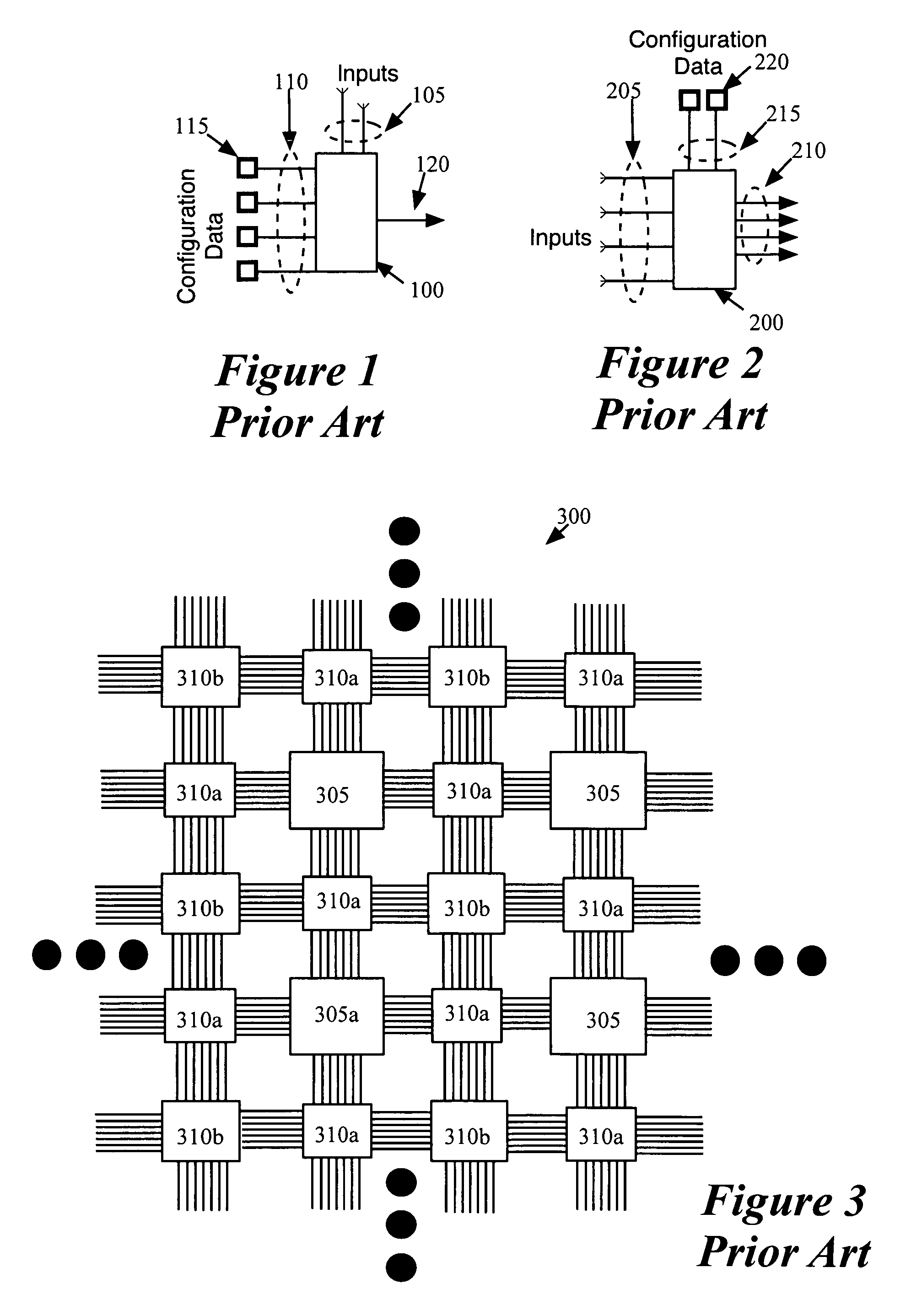
[0072]Some embodiments of the invention provide architectures for configurable IC's that have configurable computational units (e.g., configurable logic circuits) and configurable routing circuits for configurably routing signals between the configurable computational units. For instance, some embodiments provide a configurable IC that includes numerous configurable computational tiles (e.g., hundreds, thousands, hundreds of tho...


PUM


Abstract

Some embodiments of the invention provide a configurable IC that includes several configurable computational tiles and several memory tiles. These tiles are arranged in a particular tile arrangement. Each computational tile has a set of configurable logic circuits for configurably performing a plurality of computations and a set of configurable routing circuits. The routing circuits of the tiles configurably route signals between configurable logic circuits. The configurable IC also has several memory arrays for storing data on which the logic circuit perform computation. The memory arrays are embedded in the tile arrangement between two sets of memory tiles, where each set of memory tiles includes a set of routing circuits. In this IC, at least a first memory tile has the same set of configurable routing circuits as at least a second computational tile.

Description

CLAIM OF BENEFIT TO PRIOR APPLICATION[0001]This application claims benefit of an earlier-filed U.S. Provisional Patent Application 60 / 626,322, entitled “Configurable Circuits, IC's and Systems,” filed Nov. 8, 2004, which is incorporated herein by reference.CROSS REFERENCE TO RELATED APPLICATIONS[0002]This application is related to the following applications with the same filing date: U.S. patent application Ser. No. 11 / 082,193, filed Mar. 15, 2005; U.S. patent application Ser. No. 11 / 082,222, filed Mar. 15, 2005; U.S. patent application Ser. No. 11 / 082,220, filed Mar. 15, 2005; U.S. patent application Ser. No. 11 / 082,219, filed Mar. 15, 2005; U.S. patent application Ser. No. 11 / 081,867, filed Mar. 15, 2005; U.S. patent application Ser. No. 11 / 082,225, filed Mar. 15, 2005; U.S. patent application Ser. No. 11 / 081,861, filed Mar. 15, 2005; U.S. patent application Ser. No. 11 / 081,878, filed Mar. 15, 2005; and U.S. patent application Ser. No. 11 / 082,228, filed Mar. 15, 2005.FIELD OF THE ...

Claims


Application Information

Patent Timeline
IPC IPC(8): H03K19/177
CPCG11C5/025H03K19/17736H03K19/1776H01L2224/32145H01L2224/32225H01L2224/48091H01L2224/48227H01L2224/73265H01L2924/00014H01L2924/00
Inventor SCHMIT, HERMANREDGRAVE, JASON
Owner ALTERA CORP
Why Eureka
Try Eureka